- 您現(xiàn)在的位置:買賣IC網(wǎng) > PDF目錄372109 > SAA4994H (NXP SEMICONDUCTORS) Field and line rate converter with noise reduction PDF資料下載
參數(shù)資料
| 型號: | SAA4994H |
| 廠商: | NXP SEMICONDUCTORS |
| 元件分類: | 消費(fèi)家電 |
| 英文描述: | Field and line rate converter with noise reduction |
| 中文描述: | SPECIALTY CONSUMER CIRCUIT, PQFP160 |
| 封裝: | 28 X 28 MM, 3.40 MM HEIGHT, PLASTIC, MS-022, SOT-322-2, QFP-160 |
| 文件頁數(shù): | 6/40頁 |
| 文件大小: | 147K |
| 代理商: | SAA4994H |
第1頁第2頁第3頁第4頁第5頁當(dāng)前第6頁第7頁第8頁第9頁第10頁第11頁第12頁第13頁第14頁第15頁第16頁第17頁第18頁第19頁第20頁第21頁第22頁第23頁第24頁第25頁第26頁第27頁第28頁第29頁第30頁第31頁第32頁第33頁第34頁第35頁第36頁第37頁第38頁第39頁第40頁
2001 Nov 23
6
Philips Semiconductors
Product specification
Field and line rate converter
with noise reduction
SAA4994H
6
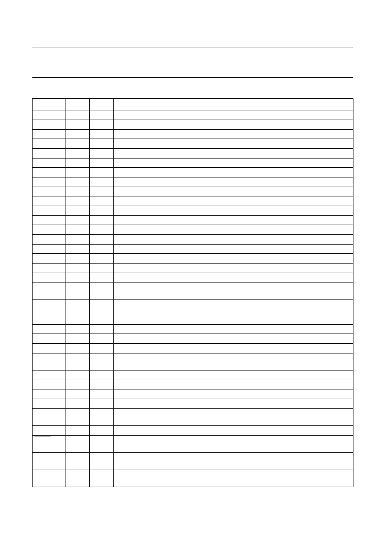
PINNING
SYMBOL
PIN
TYPE
DESCRIPTION
(1)(2)
V
SSE
YC0
YC1
YC2
YC3
YC4
YC5
YC6
YC7
UVC0
UVC1
UVC2
UVC3
REC
V
SSE
V
DDE
V
SSI
V
DDI
JUMP0
1
2
3
4
5
6
7
8
9
ground ground of output pads
input
bus C luminance input from field memory 2 bit 0 (LSB)
input
bus C luminance input from field memory 2 bit 1
input
bus C luminance input from field memory 2 bit 2
input
bus C luminance input from field memory 2 bit 3
input
bus C luminance input from field memory 2 bit 4
input
bus C luminance input from field memory 2 bit 5
input
bus C luminance input from field memory 2 bit 6
input
bus C luminance input from field memory 2 bit 7 (MSB)
input
bus C chrominance input from field memory 2 bit 0 (LSB)
input
bus C chrominance input from field memory 2 bit 1
input
bus C chrominance input from field memory 2 bit 2
input
bus C chrominance input from field memory 2 bit 3 (MSB)
output
read enable output for bus C
ground ground of output pads
supply
external supply voltage (output pads)
ground core ground
supply
core supply voltage
input
configuration pin 0; will be stored in register 0B3 e.g. to indicate presence of 3rd field
memory; should be connected to ground or to V
DDE
via a pull-up resistor of 47 k
input
configuration pin 1; will be stored in register 0B5 e.g. to indicate presence of 16-bit
1st field memory for full 4 : 2 : 2; should be connected to ground or to V
DDE
via a pull-up
resistor of 47 k
supply
external supply voltage (output pads)
supply
core supply voltage
ground core ground
input
test pin 1 input for internal RAM testing with internal pull-down; connect to ground for
normal operation
input
SNERT bus reset input
I/O
SNERT bus data input and output
input
SNERT bus clock input
ground ground of output pads
input
test pin 2 input for internal RAM testing with internal pull-down; connect to ground for
normal operation
input
test mode input with internal pull-down; if not used it has to be connected to ground
input
boundary scan test reset input (active LOW); if not used it has to be connected to V
DDE
via a pull-up resistor of 47 k
input
boundary scan test mode select input; if not used it has to be connected to V
DDE
via a
pull-up resistor of 47 k
input
boundary scan test data input; if not used it has to be connected to V
DDE
via a pull-up
resistor of 47 k
10
11
12
13
14
15
16
17
18
19
JUMP1
20
V
DDE
V
DDI
V
SSI
RAMTST1
21
22
23
24
SNRST
SNDA
SNCL
V
SSE
RAMTST2
25
26
27
28
29
TE
TRST
30
31
TMS
32
TDI
33
相關(guān)PDF資料 |
PDF描述 |
|---|---|
| SAA4998H | Field and line rate converter with noise reduction and embedded memory |
| SAA5246 | 10K OHM 0.1% 1/16W CHP RES (0603) 103 |
| SAA5246A | Integrated VIP and Teletext IVT1.0 |
| SAA5246AGP | Integrated VIP and Teletext IVT1.0 |
| SAA5246AP | Integrated VIP and Teletext IVT1.0 |
相關(guān)代理商/技術(shù)參數(shù) |
參數(shù)描述 |
|---|---|
| SAA4995WP | 制造商:PHILIPS 制造商全稱:NXP Semiconductors 功能描述:PANorama-IC PAN-IC |
| SAA4996H | 制造商:PHILIPS 制造商全稱:NXP Semiconductors 功能描述:Motion Adaptive Colour Plus And Control IC MACPACIC for PALplus |
| SAA4997H | 制造商:PHILIPS 制造商全稱:NXP Semiconductors 功能描述:VErtical Reconstruction IC VERIC for PALplus |
| SAA4998H | 制造商:PHILIPS 制造商全稱:NXP Semiconductors 功能描述:Field and line rate converter with noise reduction and embedded memory |
| SAA50 | 制造商:Anglo Adhesives 功能描述:RS STRUCT ACRYLC ADH 50ML |
發(fā)布緊急采購,3分鐘左右您將得到回復(fù)。