- 您現(xiàn)在的位置:買賣IC網(wǎng) > PDF目錄374675 > SA5230DR2 (ON SEMICONDUCTOR) Low Voltage Operational Amplifier PDF資料下載
參數(shù)資料
| 型號: | SA5230DR2 |
| 廠商: | ON SEMICONDUCTOR |
| 元件分類: | 運(yùn)動控制電子 |
| 英文描述: | Low Voltage Operational Amplifier |
| 中文描述: | OP-AMP, 4000 uV OFFSET-MAX, 0.6 MHz BAND WIDTH, PDSO8 |
| 封裝: | PLASTIC, SOP-8 |
| 文件頁數(shù): | 7/18頁 |
| 文件大?。?/td> | 253K |
| 代理商: | SA5230DR2 |
NE5230, SA5230, SE5230
http://onsemi.com
7
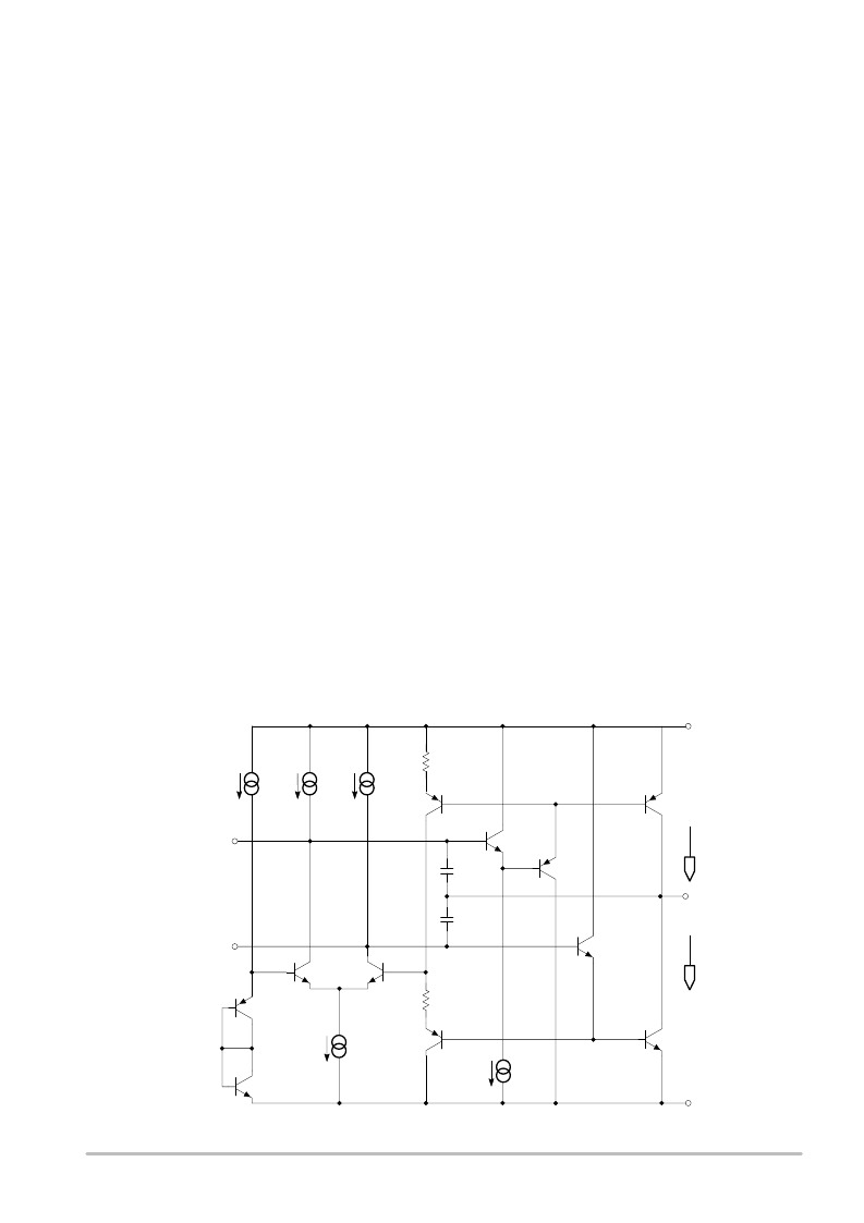
Output Stage
Processing output voltage swings that nominally reach to
less than 100 mV of either supply voltage can only be
achieved by a pair of complementary common
emitter
connected transistors. Normally, such a configuration
causes complex feed
forward signal paths that develop by
combining biasing and driving which can be found in
previous low supply voltage designs. The unique output
stage of the NE5230 separates the functions of driving and
biasing, as shown in the simplified schematic of Figure 2 and
has the advantage of a shorter signal path which leads to
increasing the effective bandwidth.
This output stage consists of two parts: the Darlington
output transistors and the class AB control regulator. The
output transistor Q3 connected with the Darlington
transistors Q4 and Q5 can source up to 10 mA to an output
load. The output of NPN Darlington connected transistors
Q1 and Q2 together are able to sink an output current of
10 mA. Accurate and efficient class AB control is necessary
to insure that none of the output transistors are ever
completely cut off. This is accomplished by the differential
amplifier (formed by Q8 and Q9) which controls the biasing
of the output transistors. The differential amplifier compares
the summed voltages across two diodes, D1 and D2, at the
base of Q8 with the summed voltages across the
base
emitter diodes of the output transistors Q1 and Q3. The
base
emitter voltage of Q3 is converted into a current by Q6
and R6 and reconverted into a voltage across the
base
emitter diode of Q7 and R7. The summed voltage
across the base
emitter diodes of the output transistors Q3
and Q1 is proportional to the logarithm of the product of the
push and pull currents I
OP
and I
ON
, respectively. The
combined voltages across diodes D1 and D2 are
proportional to the logarithm of the square of the reference
current I
B1
. When the diode characteristics and
temperatures of the pairs Q1, D1 and Q3, Q2 are equal, the
relation I
OP
×
I
ON
I
B1
×
I
B1
is satisfied.
Separating the functions of biasing and driving prevents
the driving signals from becoming delayed by the biasing
circuit. The output Darlington transistors are directly
accessible for in
phase driving signals on the bases of Q5
and Q2. This is very important for simple high
frequency
compensation. The output transistors can be high
frequency
compensated by Miller capacitors CM1A and CM1B
connected from the collectors to the bases of the output
Darlington transistors.
A general
purpose op amp of this type must have enough
open
loop gain for applications when the output is driving
a low resistance load. The NE5230 accomplishes this by
inserting an intermediate common
emitter stage between
the input and output stages. The three stages provide a very
large gain, but the op amp now has three natural dominant
poles
one at the output of each common
emitter stage.
Frequency compensation is implemented with a simple
scheme of nested, pole
splitting Miller integrators. The
Miller capacitors CM1A and CM1B are the first part of the
nested structure, and provide compensation for the output
and intermediate stages. A second pair of Miller integrators
provide pole
splitting compensation for the pole from the
input stage and the pole resulting from the compensated
combination of poles from the intermediate and output
stages. The result is a stable, internally
compensated op
amp with a phase margin of 70
°
.
Q5
I
b1
I
b2
I
b3
I
b5
I
b4
Q4
Q6
Q8
Q9
D1
Q7
Q3
D2
Q1
Q2
R7
R6
CM1B
CM1A
V
b2
V
b5
V
CC
V
EE
V
OUT
I
OP
I
ON
Figure 2. Output Stage
相關(guān)PDF資料 |
PDF描述 |
|---|---|
| SA5230DR2G | Low Voltage Operational Amplifier |
| SA5230NG | Low Voltage Operational Amplifier |
| SA5230 | Low Voltage Operational Amplifier(低壓運(yùn)算放大器) |
| SA5534A | Single Low Noise Operational Amplifier(單低噪聲運(yùn)算放大器) |
| SA5534 | Single Low Noise Operational Amplifier(單低噪聲運(yùn)算放大器) |
相關(guān)代理商/技術(shù)參數(shù) |
參數(shù)描述 |
|---|---|
| SA5230DR2G | 功能描述:運(yùn)算放大器 - 運(yùn)放 1.8V Single Rail to Rail Industrial Temp RoHS:否 制造商:STMicroelectronics 通道數(shù)量:4 共模抑制比(最小值):63 dB 輸入補(bǔ)償電壓:1 mV 輸入偏流(最大值):10 pA 工作電源電壓:2.7 V to 5.5 V 安裝風(fēng)格:SMD/SMT 封裝 / 箱體:QFN-16 轉(zhuǎn)換速度:0.89 V/us 關(guān)閉:No 輸出電流:55 mA 最大工作溫度:+ 125 C 封裝:Reel |
| SA5230FE | 制造商:PHILIPS 制造商全稱:NXP Semiconductors 功能描述:Low voltage operational amplifier |
| SA5230N | 功能描述:運(yùn)算放大器 - 運(yùn)放 1.8V Single Rail to RoHS:否 制造商:STMicroelectronics 通道數(shù)量:4 共模抑制比(最小值):63 dB 輸入補(bǔ)償電壓:1 mV 輸入偏流(最大值):10 pA 工作電源電壓:2.7 V to 5.5 V 安裝風(fēng)格:SMD/SMT 封裝 / 箱體:QFN-16 轉(zhuǎn)換速度:0.89 V/us 關(guān)閉:No 輸出電流:55 mA 最大工作溫度:+ 125 C 封裝:Reel |
| SA5230NG | 功能描述:運(yùn)算放大器 - 運(yùn)放 1.8V Single Rail to Rail Industrial Temp RoHS:否 制造商:STMicroelectronics 通道數(shù)量:4 共模抑制比(最小值):63 dB 輸入補(bǔ)償電壓:1 mV 輸入偏流(最大值):10 pA 工作電源電壓:2.7 V to 5.5 V 安裝風(fēng)格:SMD/SMT 封裝 / 箱體:QFN-16 轉(zhuǎn)換速度:0.89 V/us 關(guān)閉:No 輸出電流:55 mA 最大工作溫度:+ 125 C 封裝:Reel |
| SA5232 | 制造商:PHILIPS 制造商全稱:NXP Semiconductors 功能描述:Matched dual high-performance low-voltage operational amplifier |
發(fā)布緊急采購,3分鐘左右您將得到回復(fù)。