- 您現(xiàn)在的位置:買賣IC網(wǎng) > PDF目錄31009 > S3K/9T (VISHAY SEMICONDUCTORS) 3 A, 800 V, SILICON, RECTIFIER DIODE, DO-214AB PDF資料下載
參數(shù)資料
| 型號: | S3K/9T |
| 廠商: | VISHAY SEMICONDUCTORS |
| 元件分類: | 整流器 |
| 英文描述: | 3 A, 800 V, SILICON, RECTIFIER DIODE, DO-214AB |
| 封裝: | PLASTIC, SMC, 2 PIN |
| 文件頁數(shù): | 2/4頁 |
| 文件大?。?/td> | 335K |
| 代理商: | S3K/9T |
www.vishay.com
2
Document Number 88713
06-Sep-05
S3A thru S3M
Vishay General Semiconductor
Electrical Characteristics
(TA = 25 °C unless otherwise noted)
Thermal Characteristics
(TA = 25 °C unless otherwise noted)
Notes:
(1) Thermal resistance from junction to ambient and from junction to lead mounted on P.C.B. with 0.3 x 0.3" (8.0 x 8.0 mm) copper pad area
Ratings and Characteristics Curves
(TA = 25 °C unless otherwise noted)
Parameter
Test condition
Symbol
S3A
S3B
S3D
S3G
S3J
S3K
S3M
Unit
Maximum instantaneous forward
voltage
at 2.5 A
VF
1.15
V
Maximum DC reverse current at
rated DC blocking voltage
TA= 25 °C
TA= 125 °C
IR
10
250
A
Typical reverse recovery time
at IF = 0.5 A, IR = 1.0 A,
Irr = 0.25 A
trr
2.5
s
Typical junction capacitance
at 4.0 V, 1 MHz
CJ
60
pF
Parameter
Symbol
S3A
S3B
S3D
S3G
S3J
S3K
S3M
Unit
Typical thermal resistance (1)
RθJA
RθJL
47
13
°C/W
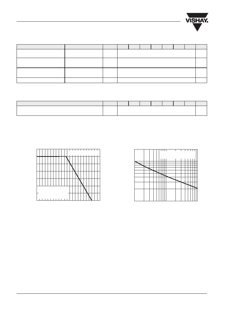
Figure 1. Forward Current Derating Curve
150
0
50
60
70
80
90 100 110 120 130 140
160
0.5
1.0
1.5
2.0
2.5
3.5
3.0
ResistiveorInductive Load
P.C.B. mounted on
0.3 x 0.3" (8.0 x 8.0mm)
Copper Pad areas
A
v
erage
F
or
w
ard
C
u
rrent
(A)
Lead Temperature (°C)
Figure 2. Maximum Non-Repetitive Peak Forward Surge Current
1
100
10
100
10
200
Number of Cycles at 60 Hz
P
eak
F
o
rw
ard
S
u
rge
C
u
rrent
(A)
TL = 75 °C
8.3 ms Single Half Sine-Wave
發(fā)布緊急采購,3分鐘左右您將得到回復(fù)。