- 您現(xiàn)在的位置:買賣IC網(wǎng) > PDF目錄374653 > S29AL016M90TFIR20 (SPANSION LLC) 16 MEGABIT (2M X 8 BIT / I M X 16 BIT) 3.0 VOLT ONLY BOOT SECTOR FLASH MEMORY PDF資料下載
參數(shù)資料
| 型號(hào): | S29AL016M90TFIR20 |
| 廠商: | SPANSION LLC |
| 元件分類: | DRAM |
| 英文描述: | 16 MEGABIT (2M X 8 BIT / I M X 16 BIT) 3.0 VOLT ONLY BOOT SECTOR FLASH MEMORY |
| 中文描述: | 1M X 16 FLASH 3V PROM, 90 ns, PDSO48 |
| 封裝: | MO-142DD, LEAD FREE, TSOP-48 |
| 文件頁(yè)數(shù): | 10/59頁(yè) |
| 文件大?。?/td> | 1917K |
| 代理商: | S29AL016M90TFIR20 |
第1頁(yè)第2頁(yè)第3頁(yè)第4頁(yè)第5頁(yè)第6頁(yè)第7頁(yè)第8頁(yè)第9頁(yè)當(dāng)前第10頁(yè)第11頁(yè)第12頁(yè)第13頁(yè)第14頁(yè)第15頁(yè)第16頁(yè)第17頁(yè)第18頁(yè)第19頁(yè)第20頁(yè)第21頁(yè)第22頁(yè)第23頁(yè)第24頁(yè)第25頁(yè)第26頁(yè)第27頁(yè)第28頁(yè)第29頁(yè)第30頁(yè)第31頁(yè)第32頁(yè)第33頁(yè)第34頁(yè)第35頁(yè)第36頁(yè)第37頁(yè)第38頁(yè)第39頁(yè)第40頁(yè)第41頁(yè)第42頁(yè)第43頁(yè)第44頁(yè)第45頁(yè)第46頁(yè)第47頁(yè)第48頁(yè)第49頁(yè)第50頁(yè)第51頁(yè)第52頁(yè)第53頁(yè)第54頁(yè)第55頁(yè)第56頁(yè)第57頁(yè)第58頁(yè)第59頁(yè)
11
S29AL016M
S29AL016M_00A4 April 21, 2004
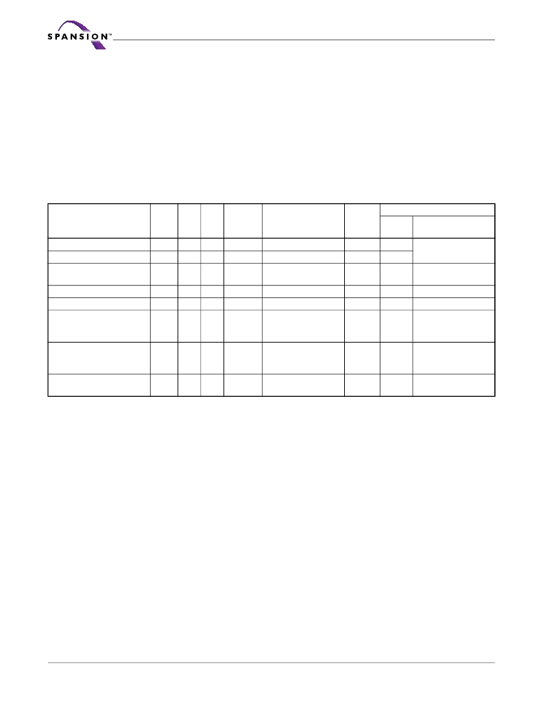
Device Bus Operations
This section describes the requirements and use of the device bus operations,
which are initiated through the internal command register. The command register
itself does not occupy any addressable memory location. The register is com-
posed of latches that store the commands, along with the address and data
information needed to execute the command. The contents of the register serve
as inputs to the internal state machine. The state machine outputs dictate the
function of the device. Table
1
lists the device bus operations, the inputs and con-
trol levels they require, and the resulting output. The following subsections
describe each of these operations in further detail.
Table 1. S29AL016M Device Bus Operations
Legend:
L = Logic Low = V
IL
, H = Logic High = V
IH
, V
ID
= 12.0
±
0.5 V, X = Don’t Care, A
IN
= Address In, D
IN
= Data In, D
OUT
= Data Out
Notes:
1. Addresses are A19:A0 in word mode (BYTE# = V
IH
), A19:A-1 in byte mode (BYTE# = V
IL
).
2. The sector protect and sector unprotect functions may also be implemented via programming equipment. See the “Sector
Protection/Unprotection” section.
Word/Byte Configuration
The BYTE# pin controls whether the device data I/O pins DQ15–DQ0 operate in
the byte or word configuration. If the BYTE# pin is set at logic ‘1’, the device is in
word configuration, DQ15–DQ0 are active and controlled by CE# and OE#.
If the BYTE# pin is set at logic ‘0’, the device is in byte configuration, and only
data I/O pins DQ0–DQ7 are active and controlled by CE# and OE#. The data I/
O pins DQ8–DQ14 are tri-stated, and the DQ15 pin is used as an input for the
LSB (A-1) address function.
Requirements for Reading Array Data
To read array data from the outputs, the system must drive the CE# and OE# pins
to V
IL
. CE# is the power control and selects the device. OE# is the output control
and gates array data to the output pins. WE# should remain at V
IH
. The BYTE#
pin determines whether the device outputs array data in words or bytes.
Operation
CE#
L
L
V
CC
±
0.3 V
L
X
OE# WE# RESET#
L
H
H
L
Addresses
(Note 1)
A
IN
A
IN
DQ0–
DQ7
D
OUT
D
IN
DQ8–DQ15
BYTE#
= V
IH
D
OUT
D
IN
BYTE#
= V
IL
Read
Write
H
H
DQ8–DQ14 = High-Z,
DQ15 = A-1
Standby
X
X
V
CC
±
0.3 V
H
L
X
High-Z
High-Z
High-Z
Output Disable
Reset
H
X
H
X
X
X
High-Z
High-Z
High-Z
High-Z
High-Z
High-Z
Sector Protect (Note 2)
L
H
L
V
ID
Sector Address,
A6 = L, A1 = H,
A0 = L
Sector Address,
A6 = H, A1 = H,
A0 = L
D
IN
X
X
Sector Unprotect (Note 2)
L
H
L
V
ID
D
IN
X
X
Temporary Sector
Unprotect
X
X
X
V
ID
A
IN
D
IN
D
IN
High-Z
相關(guān)PDF資料 |
PDF描述 |
|---|---|
| S29AL016M90TFIR22 | 16 MEGABIT (2M X 8 BIT / I M X 16 BIT) 3.0 VOLT ONLY BOOT SECTOR FLASH MEMORY |
| S29AL016M90TFIR23 | 16 MEGABIT (2M X 8 BIT / I M X 16 BIT) 3.0 VOLT ONLY BOOT SECTOR FLASH MEMORY |
| S29AL016M10FFI023 | 16 MEGABIT (2M X 8 BIT / I M X 16 BIT) 3.0 VOLT ONLY BOOT SECTOR FLASH MEMORY |
| S29AL016M10BAI013 | BCD-to-7 Segment Latch/Decoder/Driver for Liquid Crystals; Package: SOIC 16 LEAD; No of Pins: 16; Container: Tape and Reel; Qty per Container: 2500 |
| S29AL016M10BAI020 | BCD-to-7 Segment Latch/Decoder/Driver for Liquid Crystals; Package: SOEIAJ-16; No of Pins: 16; Container: Rail; Qty per Container: 50 |
相關(guān)代理商/技術(shù)參數(shù) |
參數(shù)描述 |
|---|---|
| S29AL016M90TFIR22 | 制造商:Spansion 功能描述:FLASH PARALLEL 3V/3.3V 16MBIT 2MX8/1MX16 90NS 48TSOP - Tape and Reel |
| S29AL016M90TFIR23 | 制造商:SPANSION 制造商全稱:SPANSION 功能描述:16 MEGABIT (2M X 8 BIT / I M X 16 BIT) 3.0 VOLT ONLY BOOT SECTOR FLASH MEMORY |
| S29AL032D070TFI042 | 制造商:Spansion 功能描述:32M (X8/X16) 3V, BOT BOOT, TSOP48, IND, HAZMAT, T&R - Tape and Reel |
| S29AL032D70BAI000 | 制造商:Spansion 功能描述:NOR Flash Parallel 3.3V 32Mbit 4M x 8bit 70ns 48-Pin FBGA Tray |
| S29AL032D70BAI030 | 制造商:Spansion 功能描述:NOR Flash Parallel 3V/3.3V 32Mbit 4M/2M x 8bit/16bit 70ns 48-Pin FBGA Tray |
發(fā)布緊急采購(gòu),3分鐘左右您將得到回復(fù)。