- 您現(xiàn)在的位置:買(mǎi)賣(mài)IC網(wǎng) > PDF目錄374652 > S29AL016D90TFI020 (SPANSION LLC) 16 MEGABIT CMOS 3.0 VOLT ONLY BOOT SECTOR FLASH MEMORY PDF資料下載
參數(shù)資料
| 型號(hào): | S29AL016D90TFI020 |
| 廠商: | SPANSION LLC |
| 元件分類: | DRAM |
| 英文描述: | 16 MEGABIT CMOS 3.0 VOLT ONLY BOOT SECTOR FLASH MEMORY |
| 中文描述: | 1M X 16 FLASH 3V PROM, 90 ns, PDSO48 |
| 封裝: | LEAD FREE, MO-142DDD, TSOP-48 |
| 文件頁(yè)數(shù): | 24/58頁(yè) |
| 文件大小: | 1037K |
| 代理商: | S29AL016D90TFI020 |
第1頁(yè)第2頁(yè)第3頁(yè)第4頁(yè)第5頁(yè)第6頁(yè)第7頁(yè)第8頁(yè)第9頁(yè)第10頁(yè)第11頁(yè)第12頁(yè)第13頁(yè)第14頁(yè)第15頁(yè)第16頁(yè)第17頁(yè)第18頁(yè)第19頁(yè)第20頁(yè)第21頁(yè)第22頁(yè)第23頁(yè)當(dāng)前第24頁(yè)第25頁(yè)第26頁(yè)第27頁(yè)第28頁(yè)第29頁(yè)第30頁(yè)第31頁(yè)第32頁(yè)第33頁(yè)第34頁(yè)第35頁(yè)第36頁(yè)第37頁(yè)第38頁(yè)第39頁(yè)第40頁(yè)第41頁(yè)第42頁(yè)第43頁(yè)第44頁(yè)第45頁(yè)第46頁(yè)第47頁(yè)第48頁(yè)第49頁(yè)第50頁(yè)第51頁(yè)第52頁(yè)第53頁(yè)第54頁(yè)第55頁(yè)第56頁(yè)第57頁(yè)第58頁(yè)
24
S29AL016D
S29AL016D_00_A2 December 17, 2004
P r e l i m i n a r y
Unlock Bypass Command Sequence
The unlock bypass feature allows the system to program bytes or words to the
device faster than using the standard program command sequence. The unlock
bypass command sequence is initiated by first writing two unlock cycles. This is
followed by a third write cycle containing the unlock bypass command, 20h. The
device then enters the unlock bypass mode. A two-cycle unlock bypass program
command sequence is all that is required to program in this mode. The first cycle
in this sequence contains the unlock bypass program command, A0h; the second
cycle contains the program address and data. Additional data is programmed in
the same manner. This mode dispenses with the initial two unlock cycles required
in the standard program command sequence, resulting in faster total program-
ming time.
Table 9
shows the requirements for the command sequence.
During the unlock bypass mode, only the Unlock Bypass Program and Unlock By-
pass Reset commands are valid. To exit the unlock bypass mode, the system
must issue the two-cycle unlock bypass reset command sequence. The first cycle
must contain the data 90h; the second cycle the data 00h. Addresses are don’t
care for both cycles. The device then returns to reading array data.
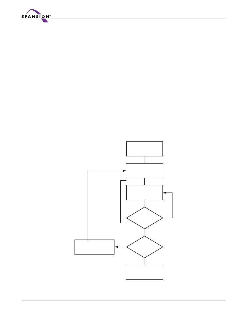
Figure 3
illustrates the algorithm for the program operation. See the
Erase/Pro-
gram Operations
table in
AC Characteristics
for parameters, and to
Figure 17
for
timing diagrams.
NOTE: See
Table 9
for program command sequence.
Figure 3. Program Operation
START
Write Program
Command Sequence
Data Poll
from System
Verify Data
No
Yes
Last Address
No
Yes
Programming
Completed
Increment Address
Embedded
Program
algorithm
in progress
相關(guān)PDF資料 |
PDF描述 |
|---|---|
| S29AL016D90TFI023 | 16 MEGABIT CMOS 3.0 VOLT ONLY BOOT SECTOR FLASH MEMORY |
| S29AL016M90FFI023 | 16 MEGABIT (2M X 8 BIT / I M X 16 BIT) 3.0 VOLT ONLY BOOT SECTOR FLASH MEMORY |
| S29AL016M | 16 MEGABIT (2M X 8 BIT / I M X 16 BIT) 3.0 VOLT ONLY BOOT SECTOR FLASH MEMORY |
| S29AL016M10 | 16 MEGABIT (2M X 8 BIT / I M X 16 BIT) 3.0 VOLT ONLY BOOT SECTOR FLASH MEMORY |
| S29AL016M10BAI010 | 16 MEGABIT (2M X 8 BIT / I M X 16 BIT) 3.0 VOLT ONLY BOOT SECTOR FLASH MEMORY |
相關(guān)代理商/技術(shù)參數(shù) |
參數(shù)描述 |
|---|---|
| S29AL016D90TFI023 | 制造商:SPANSION 制造商全稱:SPANSION 功能描述:16 MEGABIT CMOS 3.0 VOLT ONLY BOOT SECTOR FLASH MEMORY |
| S29AL016J | 制造商:SPANSION 制造商全稱:SPANSION 功能描述:16 Megabit (2 M x 8-Bit/1 M x 16-Bit) CMOS 3.0 Volt-only Boot Sector Flash Memory |
| S29AL016J55BFIR10 | 制造商:Spansion 功能描述:FLASH MEM PARALLEL 3.3V 16M-BIT 2M X 8/1M X 16 55NS TRAY - Trays |
| S29AL016J55BFNR10 | 制造商:Spansion 功能描述:FLASH MEM PARALLEL 3.3V 16M-BIT 2M X 8/1M X 16 55NS TRAY - Trays |
| S29AL016J55TFIR10 | 功能描述:閃存 16Mb 3V 55ns Parallel NOR 閃存 RoHS:否 制造商:ON Semiconductor 數(shù)據(jù)總線寬度:1 bit 存儲(chǔ)類型:Flash 存儲(chǔ)容量:2 MB 結(jié)構(gòu):256 K x 8 定時(shí)類型: 接口類型:SPI 訪問(wèn)時(shí)間: 電源電壓-最大:3.6 V 電源電壓-最小:2.3 V 最大工作電流:15 mA 工作溫度:- 40 C to + 85 C 安裝風(fēng)格:SMD/SMT 封裝 / 箱體: 封裝:Reel |
發(fā)布緊急采購(gòu),3分鐘左右您將得到回復(fù)。