- 您現(xiàn)在的位置:買賣IC網(wǎng) > PDF目錄374648 > S2202 (Applied Micro Circuits Corp.) Dual GigaBit Ethernet Transceiver(帶鎖相環(huán)時鐘合成器的雙千兆位以太網(wǎng)收發(fā)器) PDF資料下載
參數(shù)資料
| 型號: | S2202 |
| 廠商: | Applied Micro Circuits Corp. |
| 英文描述: | Dual GigaBit Ethernet Transceiver(帶鎖相環(huán)時鐘合成器的雙千兆位以太網(wǎng)收發(fā)器) |
| 中文描述: | 雙千兆以太網(wǎng)收發(fā)器(帶鎖相環(huán)時鐘合成器的雙千兆位以太網(wǎng)收發(fā)器) |
| 文件頁數(shù): | 1/28頁 |
| 文件大?。?/td> | 231K |
| 代理商: | S2202 |
當(dāng)前第1頁第2頁第3頁第4頁第5頁第6頁第7頁第8頁第9頁第10頁第11頁第12頁第13頁第14頁第15頁第16頁第17頁第18頁第19頁第20頁第21頁第22頁第23頁第24頁第25頁第26頁第27頁第28頁
1
S2202
S2202
DUAL GIGABIT ETHERNET DEVICE
October 9, 2000 / Revision C
DEVICE
SPECIFICATION
MAC
(ASIC)
S2002
DUAL
GIGABIT
ETHERNET
INTERFACE
MAC
(ASIC)
TO SERIAL BACKPLANE
S2202
GE INTERFACE
SERIAL BP DRIVER
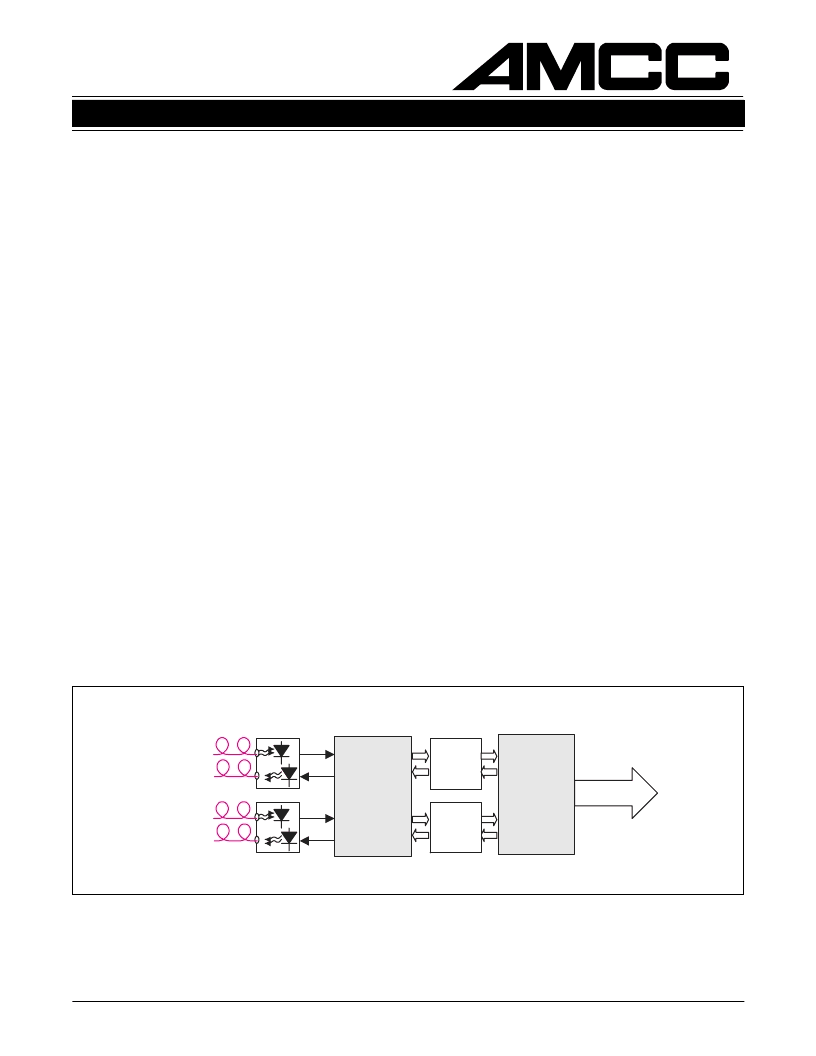
Figure 1. Typical Dual Gigabit Ethernet Application
FEATURES
1250 MHz (Gigabit Ethernet) operating rate
- Half rate operation
IEEE 802.3z Gigabit Ethernet Compatible
Dual Transmitter with phase-locked loop (PLL)
clock synthesis from low speed reference
Dual Receiver PLL provides clock and data
recovery
Internally series terminated TTL outputs
Low-jitter serial PECL interface
Individual local loopback control
JTAG 1149.1 Boundary scan on low speed I/O
signals
Interfaces with coax, twinax, or fiber optics
Single +3.3V supply, 1.85 W power dissipation
Compact 21mm x 21mm 156 TBGA package
APPLICATIONS
Ethernet Backbones
Workstation
Frame buffer
Switched networks
Data broadcast environments
Proprietary extended backplanes
GENERAL DESCRIPTION
The S2202 facilitates high-speed serial transmission
of data in a variety of applications including Gigabit
Ethernet, serial backplanes, and proprietary point to
point links. The chip provides two separate trans-
ceivers which are operated individually for a data
capacity of >2 Gbps.
Each bi-directional channel provides parallel-to-se-
rial and serial-to-parallel conversion, clock genera-
tion/recovery, and framing. The on-chip transmit PLL
synthesizes the high-speed clock from a low-speed
reference. The on-chip dual receive PLL is used for
clock recovery and data re-timing on the two inde-
pendent data inputs. The transmitter and receiver
each support differential PECL-compatible I/O for
copper or fiber optic component interfaces with ex-
cellent signal integrity. Local loopback mode allows
for system diagnostics. The chip requires a 3.3V
power supply and dissipates 1.85 watts.
Figure 1 shows the S2202 and S2002 in a Gigabit
Ethernet application. Figure 2 summarizes the in-
put/output signals of the device. Figures 3 and 4
show the transmit and receive block diagrams, re-
spectively.
相關(guān)PDF資料 |
PDF描述 |
|---|---|
| S2204 | Quad GigaBit Ethernet Transceiver(帶鎖相環(huán)時鐘合成器的四千兆位以太網(wǎng)收發(fā)器) |
| S22MD2 | Photothyristor Coupler |
| S22MD3 | MICA RoHS Compliant: No |
| S22MD1V | Silver Mica Capacitor; Capacitance:2400pF; Capacitance Tolerance:+/- 5%; Series:CM06; Voltage Rating:500VDC; Capacitor Dielectric Material:Mica; Termination:Radial Leaded; Lead Pitch:8.7mm; Leaded Process Compatible:No RoHS Compliant: No |
| S2370 | HIGH SPEED, HIGH CURRENT SWITCHING APPLICATIONS. |
相關(guān)代理商/技術(shù)參數(shù) |
參數(shù)描述 |
|---|---|
| S-2202A | 制造商:Honeywell Sensing and Control 功能描述: |
| S-2202E | 制造商:Honeywell Sensing and Control 功能描述: |
| S2202TB | 制造商:AppliedMicro 功能描述: |
| S2202TRI | 制造商:AppliedMicro 功能描述: |
| S2204TB | 制造商:AppliedMicro 功能描述:QUAD GIGABIT ETHERNET DEVICE |
發(fā)布緊急采購,3分鐘左右您將得到回復(fù)。