- 您現(xiàn)在的位置:買賣IC網(wǎng) > PDF目錄98068 > S1C63358F0A0100 4-BIT, MROM, 4.1 MHz, MICROCONTROLLER, PQFP100 PDF資料下載
參數(shù)資料
| 型號(hào): | S1C63358F0A0100 |
| 元件分類: | 微控制器/微處理器 |
| 英文描述: | 4-BIT, MROM, 4.1 MHz, MICROCONTROLLER, PQFP100 |
| 封裝: | PLASTIC, QFP15-100 |
| 文件頁(yè)數(shù): | 17/38頁(yè) |
| 文件大小: | 1226K |
| 代理商: | S1C63358F0A0100 |
第1頁(yè)第2頁(yè)第3頁(yè)第4頁(yè)第5頁(yè)第6頁(yè)第7頁(yè)第8頁(yè)第9頁(yè)第10頁(yè)第11頁(yè)第12頁(yè)第13頁(yè)第14頁(yè)第15頁(yè)第16頁(yè)當(dāng)前第17頁(yè)第18頁(yè)第19頁(yè)第20頁(yè)第21頁(yè)第22頁(yè)第23頁(yè)第24頁(yè)第25頁(yè)第26頁(yè)第27頁(yè)第28頁(yè)第29頁(yè)第30頁(yè)第31頁(yè)第32頁(yè)第33頁(yè)第34頁(yè)第35頁(yè)第36頁(yè)第37頁(yè)第38頁(yè)

14
EPSON
S1C63358 TECHNICAL MANUAL
CHAPTER 3: CPU, ROM, RAM
CHAPTER
3 CPU, ROM, RAM
3.1 CPU
The S1C63358 has a 4-bit core CPU S1C63000 built-in as its CPU part.
Refer to the "S1C63000 Core CPU Manual" for the S1C63000.
Note: The SLP instruction cannot be used because the SLEEP operation is not assumed in the S1C63358.
3.2 Code ROM
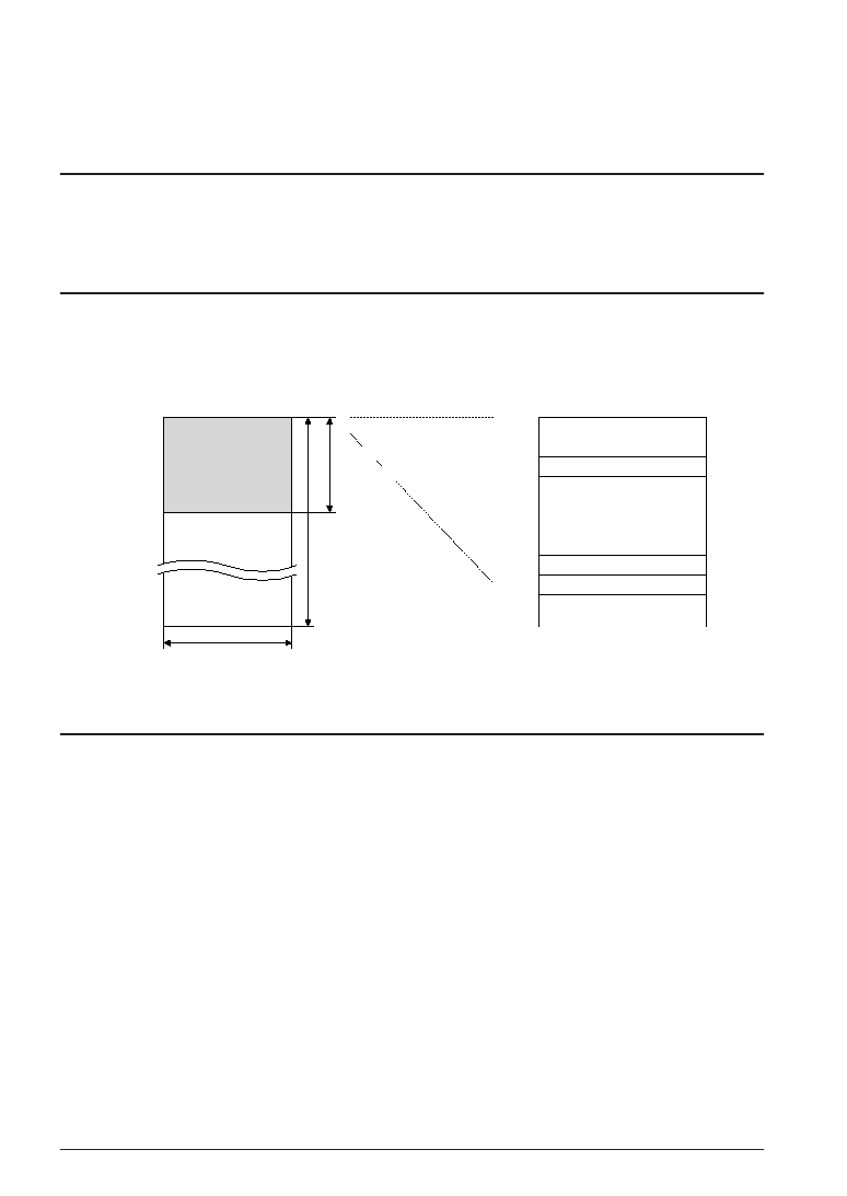
The built-in code ROM is a mask ROM for loading programs, and has a capacity of 8,192 steps
× 13 bits.
The core CPU can linearly access the program space up to step FFFFH from step 0000H, however, the
program area of the S1C63358 is step 0000H to step 1FFFH. The program start address after initial reset is
assigned to step 0110H. The non-maskable interrupt (NMI) vector and hardware interrupt vectors are
allocated to step 0100H and steps 0102H–010EH, respectively.
0000H
1FFFH
2000H
FFFFH
0000H
0100H
0102H
010EH
0110H
Program area
NMI vector
Hardware
interrupt vectors
Program start address
Program area
ROM
Unused area
13 bits
S1C63000 core CPU
program space
S1C63358
program area
Fig. 3.2.1 Configuration of code ROM
3.3 RAM
The RAM is a data memory for storing various kinds of data, and has a capacity of 512 words
× 4 bits.
The RAM area is assigned to addresses 0000H to 01FFH on the data memory map. Addresses 0100H to
01FFH are 4-bit/16-bit data accessible areas and in other areas it is only possible to access 4-bit data.
When programming, keep the following points in mind.
(1) Part of the RAM area is used as a stack area for subroutine call and register evacuation, so pay
attention not to overlap the data area and stack area.
(2) The S1C63000 core CPU handles the stack using the stack pointer for 4-bit data (SP2) and the stack
pointer for 16-bit data (SP1).
16-bit data are accessed in stack handling by SP1, therefore, this stack area should be allocated to the
area where 4-bit/16-bit access is possible (0100H to 01FFH). The stack pointers SP1 and SP2 change
cyclically within their respective range: the range of SP1 is 0000H to 01FFH and the range of SP2 is
0000H to 00FFH. Therefore, pay attention to the SP1 value because it may be set to 0200H or more
exceeding the 4-bit/16-bit accessible range in the S1C63358 or it may be set to 00FFH or less. Memory
accesses except for stack operations by SP1 are 4-bit data access.
After initial reset, all the interrupts including NMI are masked until both the stack pointers SP1 and
SP2 are set by software. Further, if either SP1 or SP2 is re-set when both are set already, the interrupts
including NMI are masked again until the other is re-set. Therefore, the settings of SP1 and SP2 must
be done as a pair.
相關(guān)PDF資料 |
PDF描述 |
|---|---|
| S1C63406F | 4-BIT, MROM, 4.2 MHz, MICROCONTROLLER, PQFP128 |
| S1C63408F0A0100 | MICROCONTROLLER, PQFP128 |
| S1C63406D0A0100 | MICROCONTROLLER, UUC103 |
| S1C63455F | 4-BIT, MROM, 4.1 MHz, MICROCONTROLLER, PQFP128 |
| S1C63455D | 4-BIT, MROM, 4.1 MHz, MICROCONTROLLER, UUC105 |
相關(guān)代理商/技術(shù)參數(shù) |
參數(shù)描述 |
|---|---|
| S1C63408 | 制造商:EPSON 制造商全稱:EPSON 功能描述:4-bit Single Chip Microcomputer |
| S1C63557D04Q000 | 制造商:Seiko Instruments Inc (SII) 功能描述:EPSON MCU 4BIT |
| S1C63567 | 制造商:EPSON 制造商全稱:EPSON 功能描述:4-bit Single Chip Microcomputer |
| S1C63616 | 制造商:EPSON 制造商全稱:EPSON 功能描述:4-bit Single Chip Microcomputer |
| S1C63632 | 制造商:EPSON 制造商全稱:EPSON 功能描述:4-bit Single Chip Microcomputer |
發(fā)布緊急采購(gòu),3分鐘左右您將得到回復(fù)。