- 您現(xiàn)在的位置:買賣IC網(wǎng) > PDF目錄374609 > S-2864B (Seiko Instruments Inc.) CMOS 64Kbit Parallel EEPROM(64K位CMOS并行EEPROM) PDF資料下載
參數(shù)資料
| 型號: | S-2864B |
| 廠商: | Seiko Instruments Inc. |
| 英文描述: | CMOS 64Kbit Parallel EEPROM(64K位CMOS并行EEPROM) |
| 中文描述: | 并行的CMOS 64Kbit的EEPROM(64K的位的CMOS并行EEPROM的) |
| 文件頁數(shù): | 9/18頁 |
| 文件大小: | 103K |
| 代理商: | S-2864B |
CMOS 64K-bit PARALLEL E
2
PROM
S-2860B/2864B
8
Seiko Instruments Inc.
Operation
(6) Write inhibition
Write operation is inhibited in the following cases :
When power supply voltage is under write inhibit voltage (V
WI
).
S-2864B : V
WI
=3.5 V typ.
S-2860B : V
WI
=2.1 V typ.
When OE is low, or WE is high.
(7) Program noise immunity
CE, OE and WE are noise protected for preventing erroneous write operation of power on and off. Less than 20 ns write
pulse will not activate a write cycle at 5-V opeation, and less than 50 ns at 3-V operation. See Figure 9.
(1) Read mode
This mode outputs data to I/O
0
to I/O
7
when both CE and OE are low and when WE is high. The data bus is high impedance
when either CE or OE is high.
(2) Byte write mode
A byte write cycle starts when both CE and WE are low and OE is high. CE-and WE-controlled write cycles are available.
The address is latched at the falling of CE or WE whichever occurs last, and the data is latched at the rising of CE or WE
whichever occurs first.
(3) Page write mode
In this mode, 1 page program operation of 32 bytes is completed in 10 ms, and all memory area is written within 3 second
because the device organization is 256-page
×
32-byte. When starting this mode, first, addresses A
5
to A
12
assign the page,
then A
0
to A
4
assign the address to each byte within the page sequencially or at random. Less than 32 bytes of program is
available. This address assignment is performed while 0.3
μ
s
≤
t
PL
≤
30
μ
s, and the program operation starts when t
PDL
≥
100
μ
s.
(4) Data polling
This function is to output the complement data written last on I/O
7
and to output low to I/O
0
to I/O
6
. This operation is
performed by read operation during write cycle.
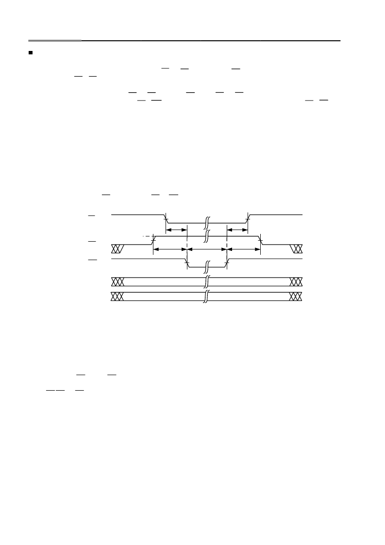
(5) Erase all mode
All data is erased when OE is 13 V and both CE and WE are low. During erase all mode, A
0
to A
12
and I/O
0
to I/O
7
must be
fixed to either high or low.
Figure 8
I/O
Address
WE
OE
CE
13 V
100 ns min.
100 ns min.
10 ms min.
1
μ
s min.
1
μ
s min.
相關(guān)PDF資料 |
PDF描述 |
|---|---|
| S-2900ACA | CMOS 512-bit SERIAL EEPROM |
| S-2900ADP | CMOS 512-bit SERIAL EEPROM |
| S-2900AFE | CMOS 512-bit SERIAL EEPROM |
| S-2900AUP | CMOS 512-bit SERIAL EEPROM |
| S-2900A | CMOS 512Bit Serial EEPROM(512位 CMOS 串行EEPROM) |
相關(guān)代理商/技術(shù)參數(shù) |
參數(shù)描述 |
|---|---|
| S2865AG2NRF-RS | 制造商:TYAN 功能描述:FULLY-LOADED, PCIE X16, ROHS - Bulk |
| S2865ANRF | 制造商:TYAN 功能描述:DESKTOP, PCIE X16 - Trays |
| S2865G2NR | 制造商:TYAN 功能描述:SERVER, PCIE X16, DUAL LAN - Trays |
| S2865G2NR RPL | 制造商:TYAN 功能描述:REPAIR/REPLACEMENT - Bulk |
| S2865G2NR-DF | 制造商:TYAN 功能描述:TOMCAT K8E NFORCE4 BOARD - Bulk |
發(fā)布緊急采購,3分鐘左右您將得到回復(fù)。