- 您現(xiàn)在的位置:買賣IC網(wǎng) > PDF目錄66151 > RX-8025NBAA-3 REAL TIME CLOCK, PDSO22 PDF資料下載
參數(shù)資料
| 型號: | RX-8025NBAA-3 |
| 元件分類: | 時鐘/數(shù)據(jù)恢復(fù)及定時提取 |
| 英文描述: | REAL TIME CLOCK, PDSO22 |
| 封裝: | SON-22 |
| 文件頁數(shù): | 2/3頁 |
| 文件大小: | 270K |
| 代理商: | RX-8025NBAA-3 |
87
Real time clock module
88
Real time clock module
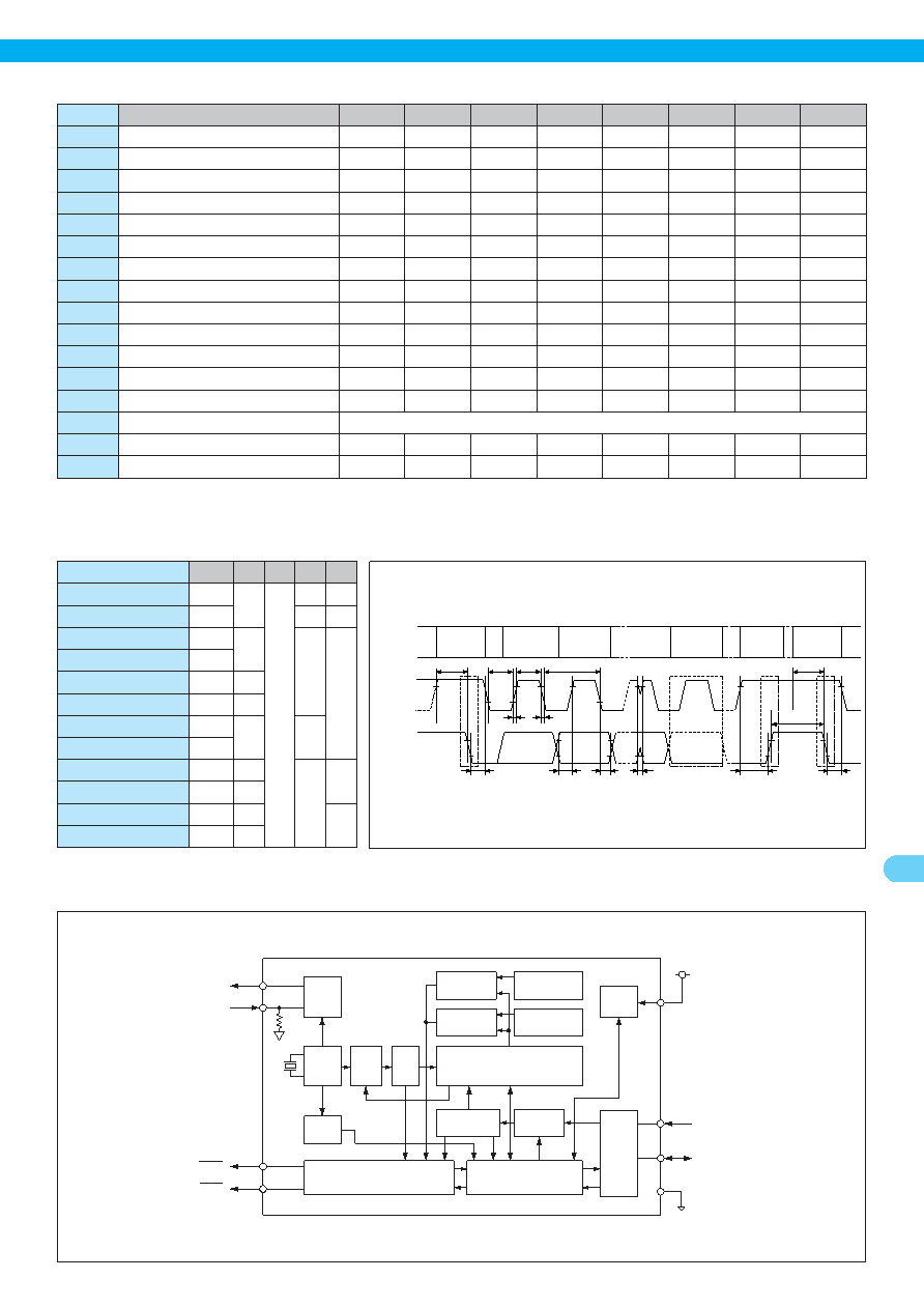
Register table
Address
Register symbol
bit 7
bit 6
bit 5
bit 4
bit 3
bit 2
bit 1
bit 0
0
Seconds
o
S 40
S 20
S 10
S 8
S 4
S 2
S 1
1
Minutes
o
M 40
M 20
M 10
M 8
M 4
M 2
M 1
2
Hours
o
H 20 P, A
__
H 10
H 8
H 4
H 2
H 1
3
Weekdays
o
W 4
W 2
W 1
4
Days
o
D 20
D 10
D 8
D 4
D 2
D 1
5
Months
o
MO 10
MO 8
MO 4
MO 2
MO 1
6
Years
Y 80
Y 40
Y 20
Y 10
Y 8
Y 4
Y 2
Y 1
7
Digital Offset
o
F 6
F 5
F 4
F 3
F 2
F 1
F 0
8
Alarm_W ; Minutes
o
WM 40
WM 20
WM 10
WM 8
WM 4
WM 2
WM 1
9
Alarm_W ; Hour
o
WH 20 WP, A
WH 10
WH 8
WH 4
WH 2
WH 1
A
Alarm_W ; Weekday
o
WW 6
WW 5
WW 4
WW 3
WW 2
WW 1
WW 0
B
Alarm_D ; Minutes
o
DM 40
DM 20
DM 10
DM 8
DM 4
DM 2
DM 1
C
Alarm_D ; Hour
o
DH 20 DP, A
__
DH 10
DH 8
DH 4
DH 2
DH 1
D
Reserved
E
Control 1
WALE
DALE
1
____
2, 24
C
___________
LEN 2
TEST
CT 2
CT 1
CT 0
F
Control 2
VDSL
VDET
X
______
ST
PON
C
___________
LEN 1
CTFG
WAFG
DAFG
0 : Always set this bit to “0”.
AC characteristics
Item
Symbol Min. Typ. Max. Unit
SCL clock frequency
fSCL
–
400 kHz
Tolerance spike time on bus
tSP
50
ns
Start condition set-up time tSU ; STA
0.6
s
Start condition Hold time
tHD ; STA
SCL “L” time
tLOW
1.3
SCL “H” time
tHIGH
0.6
SCL and SDA rise time
tr
–
0.3
SCL and SDA fall time
tf
Data set-up time
tSU ; DAT 200
ns
Data hold time
tHD ; DAT
0
Stop condition set-up time tSU ; STO 0.6
s
Bus free time
tBUF
2.0
Timing chart
Protocol
SCL
Start
Condition (s)
Start
Condition (s)
Stop
Condition (P)
tSU;STO
tSP
tHD;DAT
tSU;STA
tHD;STA
tSU;STA
tLOW
tHIGH
1/fSCL
(A)
(P)
(S)
tf
tr
(S)
tBUF
tSU;DAT
tHD;STA
Bit 7
MSB (A7)
Bit6
(A6)
Bit0
LSB
(R/W)
ACK
(A)
SDA
Block diagram
INTA
FOUT
VDD
FOE
SCL
SDA
GND
INTB
OSC
Interrupt Control
Shift Register
Time Counter
(Sec, Min, Hour, Week, Day, Month,Year)
I/O
Control
Voltage
Detect
Div.
Divider
Correc
-tion
32 kHz
Output
Control
OSC
Detect
Address
Decoder
Alarm_D Register
(Min, Hour)
Comparator_D
Comparator_W
Address
Register
Alarm_W Register
(Min, Hour, Week)
相關(guān)PDF資料 |
PDF描述 |
|---|---|
| RX-8025NBAA-0 | REAL TIME CLOCK, PDSO22 |
| RX-8025SAAA-3 | REAL TIME CLOCK, PDSO14 |
| RX-8571LC | REAL TIME CLOCK, PDSO12 |
| RX-8571NB | REAL TIME CLOCK, PDSO22 |
| RX-8581JEB-0 | REAL TIME CLOCK, PDSO20 |
相關(guān)代理商/技術(shù)參數(shù) |
參數(shù)描述 |
|---|---|
| RX-8025SA | 制造商:Epson Toyocom Corporation 功能描述:32.768kHz 0.48uA@3V(Typ.) 1.7 to 5.5V 10.1~5.0~3.2mm +85 -40 5}23ppm@+25/3.0V I2C-BusVAC^[tFCX 10.1mm 5mm 3.2mm 制造商:Epson Toyocom 功能描述:RTC module,I2C Bus,High Stability,SOP14 |
| RX-8025SA AA | 制造商:Epson Electronics America Inc 功能描述:Real Time Clock Serial 14-Pin SOP Bulk |
發(fā)布緊急采購,3分鐘左右您將得到回復(fù)。