- 您現(xiàn)在的位置:買賣IC網(wǎng) > PDF目錄374589 > RFP2N12L (HARRIS SEMICONDUCTOR) 2A, 120V, 1.750 Ohm, Logic Level,N-Channel Power MOSFET(2A, 120V,1.750 Ω, N溝道,邏輯電平,功率MOS場效應(yīng)管) PDF資料下載
參數(shù)資料
| 型號: | RFP2N12L |
| 廠商: | HARRIS SEMICONDUCTOR |
| 元件分類: | JFETs |
| 英文描述: | 2A, 120V, 1.750 Ohm, Logic Level,N-Channel Power MOSFET(2A, 120V,1.750 Ω, N溝道,邏輯電平,功率MOS場效應(yīng)管) |
| 中文描述: | 2 A, 120 V, 1.75 ohm, N-CHANNEL, Si, POWER, MOSFET, TO-220AB |
| 文件頁數(shù): | 2/5頁 |
| 文件大小: | 35K |
| 代理商: | RFP2N12L |
6-253
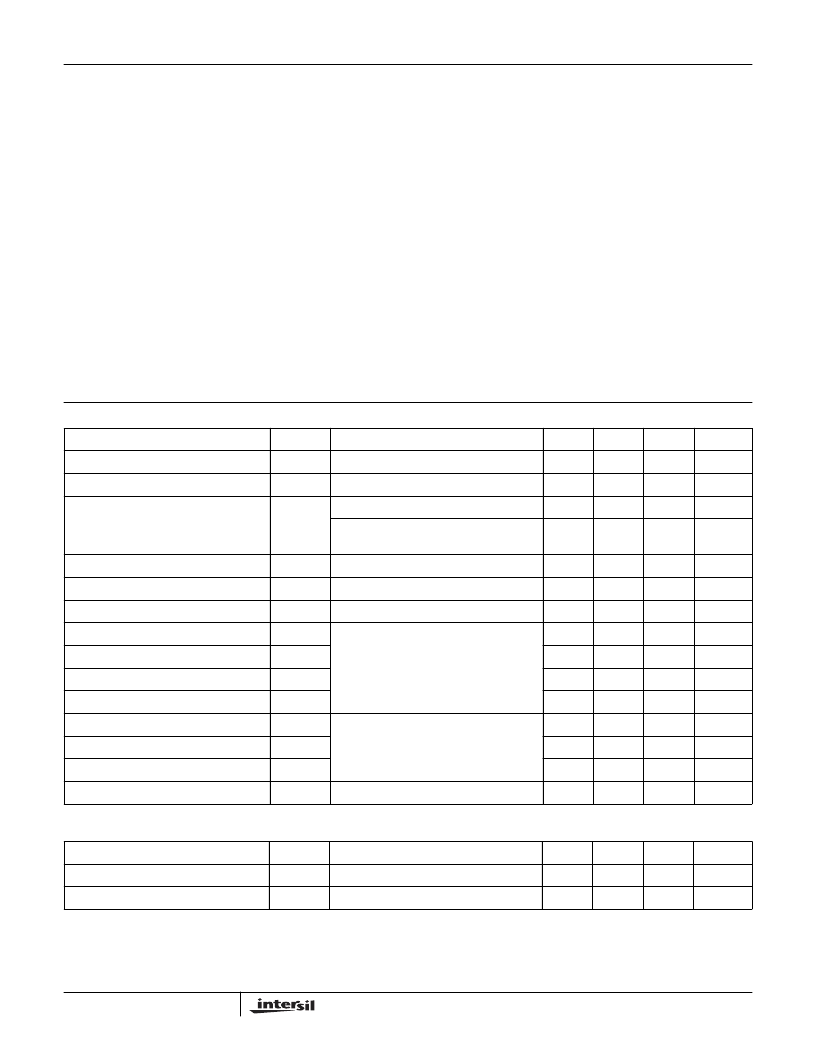
Absolute Maximum Ratings
T
C
= 25
o
C, Unless Otherwise Specified
RFP2N12L
UNITS
Drain to Source Voltage (Note 1). . . . . . . . . . . . . . . . . . . . . . . . . . . . . . . . . . . . . . . . . . . . . . . V
DSS
Drain to Gate Voltage RGS = 20K
(Note 1). . . . . . . . . . . . . . . . . . . . . . . . . . . . . . . . . . . . . . V
DGR
Gate to Source Voltage . . . . . . . . . . . . . . . . . . . . . . . . . . . . . . . . . . . . . . . . . . . . . . . . . . . . . . . V
GS
Continuous Drain Current . . . . . . . . . . . . . . . . . . . . . . . . . . . . . . . . . . . . . . . . . . . . . . . . . . . . . . . I
D
Pulsed Drain Current (Note 3) . . . . . . . . . . . . . . . . . . . . . . . . . . . . . . . . . . . . . . . . . . . . . . . . .I
DM
Maximum Power Dissipation . . . . . . . . . . . . . . . . . . . . . . . . . . . . . . . . . . . . . . . . . . . . . . . . . . . . P
D
Derate Above T
C
= 25
o
C . . . . . . . . . . . . . . . . . . . . . . . . . . . . . . . . . . . . . . . . . . . . . . . . . . . . . . . .
Operating and Storage Temperature . . . . . . . . . . . . . . . . . . . . . . . . . . . . . . . . . . . . . . . . . T
J
, T
STG
Maximum Temperature for Soldering
Leads at 0.063in (1.6mm) from Case for 10s. . . . . . . . . . . . . . . . . . . . . . . . . . . . . . . . . . . . . . .T
L
Package Body for 10s, See Techbrief 334 . . . . . . . . . . . . . . . . . . . . . . . . . . . . . . . . . . . . . . . T
pkg
120
V
120
V
±
10
V
2
A
5
A
25
W
0.2
W/
o
C
o
C
-55 to 150
300
260
o
C
o
C
CAUTION: Stresses above those listed in “Absolute Maximum Ratings” may cause permanent damage to the device. This is a stress only rating and operation of the
device at these or any other conditions above those indicated in the operational sections of this specification is not implied.
NOTE:
1. T
J
= 25
o
C to 125
o
C.
Electrical Specifications
T
C
= 25
o
C, Unless Otherwise Specified
PARAMETER
SYMBOL
TEST CONDITIONS
MIN
TYP
MAX
UNITS
Drain to Source Breakdown Voltage
BV
DSS
I
D
= 250
μ
A, V
GS
= 0
120
-
-
V
Gate to Threshold Voltage
V
GS(TH)
V
GS
= V
DS
, I
D
= 250
μ
A (Figure 8)
1
-
2
V
Zero-Gate Voltage Drain Current
I
DSS
V
DS
= Rated BV
DSS
, V
GS
= 0V
-
-
1
μ
A
V
DS
= 0.8 x Rated BV
DSS
, V
GS
= 0V,
T
C
= 125
o
C
-
-
25
μ
A
Gate to Source Leakage Current
I
GSS
V
GS
=
±
10V, V
DS
= 0V
-
-
±
100
nA
Drain to Source On Voltage (Note 2)
V
DS(ON)
I
D
= 2A, V
GS
= 5V
-
-
3.5
V
Drain to Source On Resistance (Note 2)
r
DS(ON)
I
D
= 2A, V
GS
= 5V (Figure 6, 7)
-
-
1.750
Turn-On Delay Time
t
d(ON)
I
D
≈
2A, V
DD
= 75V, R
G
= 6.25
,
R
L
= 75
, V
GS
= 5V
(Figures 10, 11, 12)
-
10
25
ns
Rise Time
t
r
-
10
45
ns
Turn-Off Delay Time
t
d(OFF)
-
24
45
ns
Fall Time
t
f
-
20
25
ns
Input Capacitance
C
ISS
V
GS
= 0V, V
DS
= 25V, f = 1MHz
(Figure 9)
-
-
200
pF
Output Capacitance
C
OSS
-
-
80
pF
Reverse Transfer Capacitance
C
RSS
-
-
35
pF
Thermal Resistance Junction to Case
R
θ
JC
-
-
5
o
C/W
Source to Drain Diode Specifications
PARAMETER
SYMBOL
TEST CONDITIONS
MIN
TYP
MAX
UNITS
Source to Drain Diode Voltage (Note 2)
V
SD
I
SD
= 2A
-
-
1.4
V
Diode Reverse Recovery Time
t
rr
I
SD
= 2A, dl
SD
/dt = 50A/
μ
s
-
150
-
ns
NOTES:
2. Pulsed: pulse duration = 300
μ
s max, duty cycle = 2%.
3. Repetitive rating: pulse width limited by maximum junction temperature.
RFP2N12L
相關(guān)PDF資料 |
PDF描述 |
|---|---|
| RFP2N12 | 2A, 120V and 150V, 1.750 Ohm, N-Channel Power MOSFETs |
| RFP2N15 | 2A, 120V and 150V, 1.750 Ohm, N-Channel Power MOSFETs |
| RFP2N20L | 2A, 200V, 3.500 Ohm, Logic Level, N-Channel Power MOSFET |
| RFP2N20 | 2A, 200V, 3.500 Ohm, N-Channel Power MOSFET |
| RFP2P08 | -2A, -80V and -100V, 3.500 Ohm, P-Channel Power MOSFETs |
相關(guān)代理商/技術(shù)參數(shù) |
參數(shù)描述 |
|---|---|
| RFP2N15 | 制造商:Rochester Electronics LLC 功能描述:- Bulk 制造商:RCA 功能描述:MOSFET 制造商:Harris Corporation 功能描述: |
| RFP2N15L | 制造商:未知廠家 制造商全稱:未知廠家 功能描述:TRANSISTOR | MOSFET | N-CHANNEL | 150V V(BR)DSS | 2A I(D) | TO-220AB |
| RFP2N18 | 制造商:Harris Corporation 功能描述: |
| RFP2N18L | 制造商:未知廠家 制造商全稱:未知廠家 功能描述:TRANSISTOR | MOSFET | N-CHANNEL | 180V V(BR)DSS | 2A I(D) | TO-220AB |
| RFP2N20 | 制造商:Rochester Electronics LLC 功能描述:- Bulk 制造商:Harris Corporation 功能描述: |
發(fā)布緊急采購,3分鐘左右您將得到回復(fù)。