- 您現(xiàn)在的位置:買賣IC網(wǎng) > PDF目錄374589 > RFP25N05 (Electronic Theatre Controls, Inc.) POWER MOS FIELD EFFECT TRANSISTORS PDF資料下載
參數(shù)資料
| 型號(hào): | RFP25N05 |
| 廠商: | Electronic Theatre Controls, Inc. |
| 英文描述: | POWER MOS FIELD EFFECT TRANSISTORS |
| 中文描述: | 功率MOS場(chǎng)效應(yīng)晶體管 |
| 文件頁(yè)數(shù): | 2/8頁(yè) |
| 文件大?。?/td> | 104K |
| 代理商: | RFP25N05 |
4-505
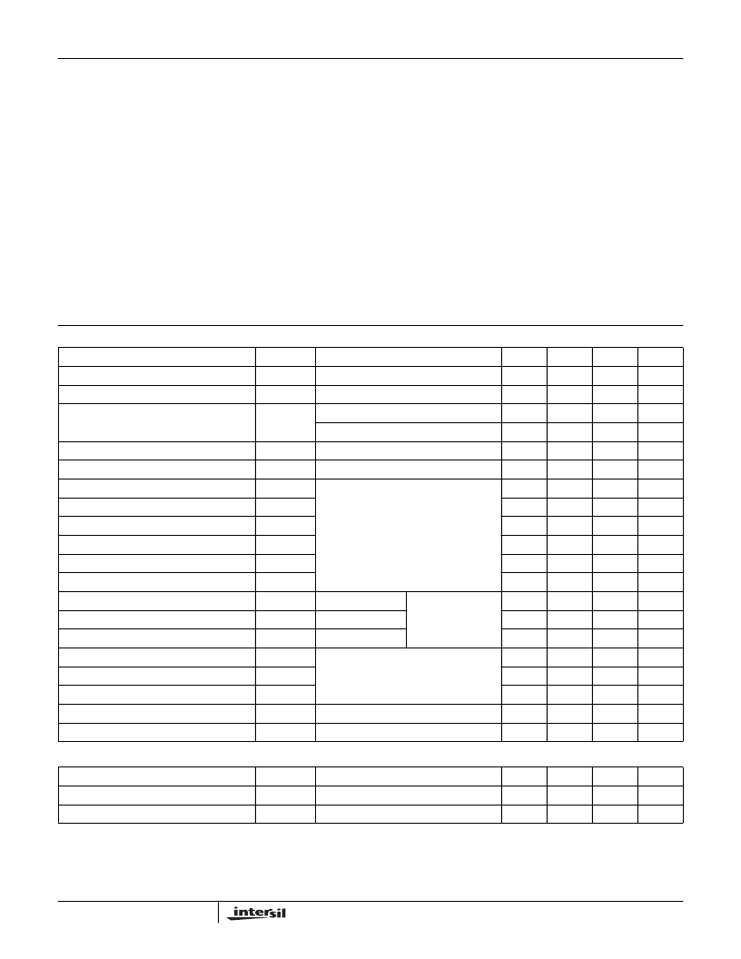
Absolute Maximum Ratings
T
C
= 25
o
C, Unless Otherwise Specified
RFP25N05
50
50
±
20
25
UNITS
V
V
V
A
A
Drain to Source Voltage (Note 1). . . . . . . . . . . . . . . . . . . . . . . . . . . . . . . . . . . . . . . . . . V
DSS
Drain to Gate Voltage . . . . . . . . . . . . . . . . . . . . . . . . . . . . . . . . . . . . . . . . . . . . . . . . . .V
DGR
Gate to Source Voltage . . . . . . . . . . . . . . . . . . . . . . . . . . . . . . . . . . . . . . . . . . . . . . . . . . V
GS
Continuous Drain Current . . . . . . . . . . . . . . . . . . . . . . . . . . . . . . . . . . . . . . . . . . . . . . . . . . I
D
Pulsed Drain Current (Note 3) . . . . . . . . . . . . . . . . . . . . . . . . . . . . . . . . . . . . . . . . . . . . . .I
DM
Pulsed Avalanche Rating. . . . . . . . . . . . . . . . . . . . . . . . . . . . . . . . . . . . . . . . . . . . . . . . . E
AS
Maximum Power Dissipation . . . . . . . . . . . . . . . . . . . . . . . . . . . . . . . . . . . . . . . . . . . . . . . P
D
Linear Derating Factor . . . . . . . . . . . . . . . . . . . . . . . . . . . . . . . . . . . . . . . . . . . . . . . . . . . . . . .
Operating and Storage Temperature . . . . . . . . . . . . . . . . . . . . . . . . . . . . . . . . . . . . T
J
, T
STG
Maximum Temperature for Soldering
Leads at 0.063in (1.6mm) from Case for 10s. . . . . . . . . . . . . . . . . . . . . . . . . . . . . . . . . .T
L
Package Body for 10s, See Techbrief 334 . . . . . . . . . . . . . . . . . . . . . . . . . . . . . . . . . . T
pkg
CAUTION: Stresses above those listed in “Absolute Maximum Ratings” may cause permanent damage to the device. This is a stress only rating and operation of the
device at these or any other conditions above those indicated in the operational sections of this specification is not implied.
Refer to Peak Current Curve
Refer to UIS Curve
72
0.48
-55 to 175
W
W/
o
C
o
C
300
260
o
C
o
C
NOTE:
1. T
J
= 25
o
C to 150
o
C.
Electrical Specifications
T
C
= 25
o
C, Unless Otherwise Specified
PARAMETER
SYMBOL
TEST CONDITIONS
MIN
TYP
MAX
UNITS
Drain to Source Breakdown Voltage
BV
DSS
I
D
= 250
μ
A, V
GS
= 0V (Figure 11)
50
-
-
V
Gate Threshold Voltage
V
GS(TH)
V
GS
= V
DS
, I
D
= 250mA (Figure 10)
2
-
4
V
Zero Gate Voltage Drain Current
I
DSS
V
DS
= Rated BV
DSS
, V
GS
= 0V
V
DS
= 0.8 x Rated BV
DSS
,T
C
= 150
o
C
V
GS
=
±
20V
-
-
1
μ
A
-
-
25
μ
A
Gate to Source Leakage Current
I
GSS
-
-
±
100
nA
Drain to Source On Resistance
r
DS(ON)
I
D
= 25A, V
GS
= 10V (Figure 9)
V
DD
= 25V, I
D
≈
12.5A, R
L
= 2.0
,
V
GS
= 10V, R
G
= 10
(Figure 13)
-
-
0.047
Turn-On Time
t
ON
-
-
60
ns
Turn-On Delay Time
t
d(ON)
-
14
-
ns
Rise Time
t
r
-
30
-
ns
Turn-Off Delay Time
t
d(OFF)
-
45
-
ns
Fall Time
t
f
-
22
-
ns
Turn-Off Time
t
OFF
-
-
100
ns
Total Gate Charge
Q
G(TOT)
V
GS
= 0V to 20V
V
DD
= 40V,
I
D
= 25A, R
L
= 1.6
I
g(REF)
= 0.75mA
(Figure 13)
-
-
80
nC
Gate Charge at 10V
Q
G(10)
V
GS
= 0V to 10V
-
-
45
nC
Threshold Gate Charge
Q
G(TH)
V
GS
= 0V to 2V
-
-
3
nC
Input Capacitance
C
ISS
V
DS
= 25V, V
GS
= 0V,
f = 1MHz
(Figure 12)
-
1075
-
pF
Output Capacitance
C
OSS
-
350
-
pF
Reverse Transfer Capacitance
C
RSS
-
100
-
pF
Thermal Resistance Junction to Case
R
θ
JC
R
θ
JA
(Figure 3)
-
-
2.083
o
C/W
Thermal Resistance Junction to Ambient
-
-
80
o
C/W
Source to Drain Diode Specifications
PARAMETER
SYMBOL
TEST CONDITIONS
MIN
TYP
MAX
UNITS
Source to Drain Diode Voltage (Note 2)
V
SD
I
SD
= 25A
I
SD
= 25A, dI
SD
/dt = 100A/
μ
s
-
-
1.5
V
Reverse Recovery Time
t
RR
-
-
125
ns
NOTES:
2. Pulse test: pulse width
≤
300
μ
s, duty cycle
≤
2%.
3. Repetitive rating: pulse width limited by maximum junction temperature. See Transient Thermal Impedance curve (Figure 3) and Peak Current
Capability Curve (Figure 5).
RFP25N05
相關(guān)PDF資料 |
PDF描述 |
|---|---|
| RFP25N06 | POWER MOS FIELD EFFECT TRANSISTORS |
| RFP25N06 | 25A, 60V, 0.047 Ohm, N-Channel Power MOSFETs |
| RFP25N06 | 25A, 60V, 0.047 Ohm, N-Channel Power MOSFETs |
| RFP2N08L | 2A, 80V, 0.140 Ohm, Logic Level,N-Channel Power MOSFET(2A, 80V, 0.140 Ω, N溝道,邏輯電平,功率MOS場(chǎng)效應(yīng)管) |
| RFP2N10L | 2A, 80V and 100V, 1.050 Ohm, Logic Level, N-Channel Power MOSFETs |
相關(guān)代理商/技術(shù)參數(shù) |
參數(shù)描述 |
|---|---|
| RFP25N05L | 制造商:Harris Corporation 功能描述: |
| RFP25N06 | 制造商:INTERSIL 制造商全稱:Intersil Corporation 功能描述:25A, 60V, 0.047 Ohm, N-Channel Power MOSFETs |
| RFP25N06L | 制造商:Rochester Electronics LLC 功能描述:- Bulk 制造商:Harris Corporation 功能描述: |
| RFP2N08 | 制造商:Rochester Electronics LLC 功能描述:- Bulk 制造商:Harris Corporation 功能描述: |
| RFP2N08L | 制造商:INTERSIL 制造商全稱:Intersil Corporation 功能描述:2A, 80V and 100V, 1.050 Ohm, Logic Level, N-Channel Power MOSFETs |
發(fā)布緊急采購(gòu),3分鐘左右您將得到回復(fù)。