- 您現(xiàn)在的位置:買賣IC網(wǎng) > PDF目錄373262 > RF2431 RF Mixer PDF資料下載
參數(shù)資料
| 型號(hào): | RF2431 |
| 英文描述: | RF Mixer |
| 中文描述: | RF混頻器 |
| 文件頁(yè)數(shù): | 4/10頁(yè) |
| 文件大小: | 146K |
| 代理商: | RF2431 |
8-46
RF2431
Rev B1 010329
8
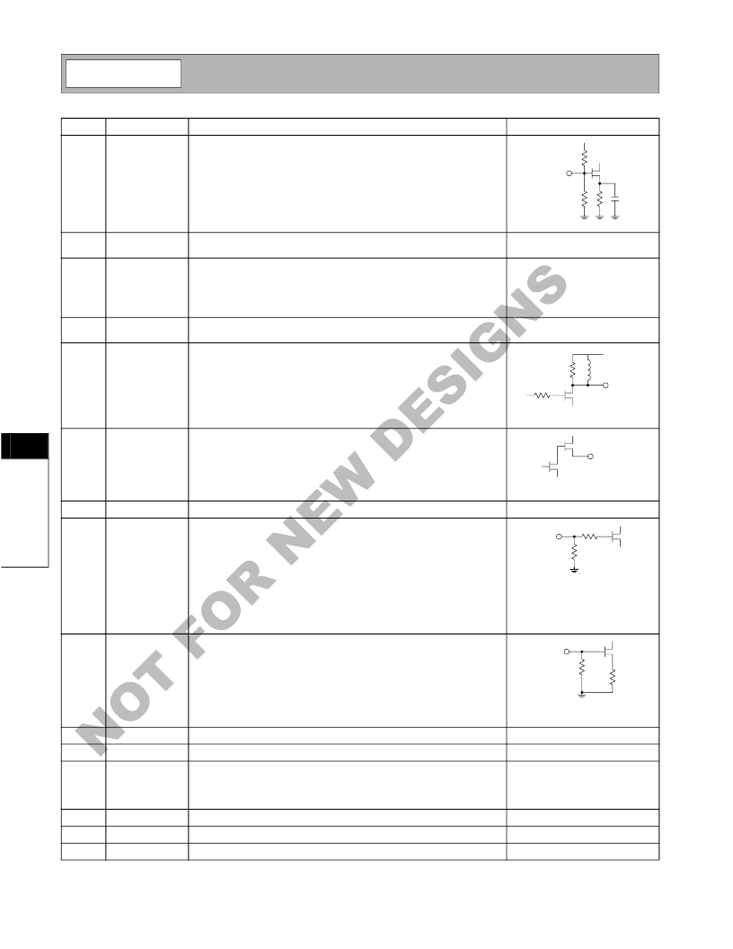
F
Pin
1
Function
LNA IN
Description
This pin is NOT internally DC blocked. An external blocking capacitor
must be provided if the pin is connected to a device with DC present. A
DC path to ground (i.e. an inductor or resistor to ground) is, however,
acceptable at this pin. If a blocking capacitor is required, a value of
22pF is recommended.
Interface Schematic
2
GND
Ground connection. Keep traces physically short and connect immedi-
ately to ground plane for best performance.
Supply voltage for the LNA only. A 22pF external bypass capacitor is
required and an additional 0.01
μ
F is required if no other low frequency
bypass capacitors are nearby. The trace length between the pin and the
bypass capacitors should be minimized. The ground side of the bypass
capacitors should connect immediately to ground plane.
Power supply for the IF buffer amplifier. If the high impedance mixer
output is being used, then this pin is not connected.
Open drain output port, one of the two output options. This pin must be
connected to V
DD
through a resistor in order to bias the mixer, even
when using the IF2 Output. In addition, a 0.1
μ
F bypass capacitor is
required at the other end of the bias resistor. This output is intended to
drive high impedance IF filters. The intrinsic output impedance is about
4k
, which means that the actual impedance is set by the external
resistor to V
DD
.
50
buffered output port, one of the two output options. This is an
open drain output, therefore a resistor to ground is needed. The typical
value for this resistor is 470
. Pin 4 must be connected to V
DD
in order
to turn the buffer amplifier on. Current drain will increase by approxi-
mately 6mA at 5V; by approximately 3mA at 3V.This pin is not con-
nected when using the high impedance port.
Same as pin 2.
3
VDD1
4
VDD2
5
IF1 OUT
6
IF2 OUT
7
8
GND
LO IN
Mixer LO input. An high-pass matching network, such as a single shunt
inductor (as shown in the application schematics), is the recommended
topology because it also rejects IF noise at the mixer input. The value
of this inductor is depending on the frequency, see the application
schematics. This filtering is required to achieve the specified noise fig-
ures. This pin is NOT internally DC blocked. An external blocking
capacitor must be provided if the pin is connected to a device with DC
present. A DC path to ground (i.e. an inductor or resistor to ground) is,
however, acceptable at this pin. If a blocking capacitor is required, a
value of 22pF is recommended.
Mixer RF Input port. This pin is NOT internally DC blocked. An external
blocking capacitor must be provided if the pin is connected to a device
with DC present. A DC path to ground (i.e. an inductor or resistor to
ground) is, however, acceptable at this pin. If a blocking capacitor is
required, a value of 22pF is recommended. Matching is required; see
the applications schematics.To minimize the noise figure it is recom-
mended to have a bandpass filter before this input. This will prevent the
noise at the image frequency from being converted to the IF.
Same as pin 2.
9
RF IN+
10
11
12
GND
NC
RF BYP
No connection
Connection for the external bypass capacitor for the mixer input buffer
amplifier. 1nF is recommended. The trace length between the pin and
the capacitor should be minimized. The ground side of the bypass
capacitor should connect immediately to ground plane.
No connection.
13
14
15
NC
NC
GND
No connection.
Same as pin 2.
LNA IN
IF1 OUT
IF2 OUT
LO IN
RF IN
相關(guān)PDF資料 |
PDF描述 |
|---|---|
| RF2450 | Analog IC |
| RF2454 | RF Modulator |
| RF2464 | RF Modulator |
| RF24 | Analog IC |
| RF250 | Quadrature Demodulator |
相關(guān)代理商/技術(shù)參數(shù) |
參數(shù)描述 |
|---|---|
| RF2432-000 | 功能描述:可復(fù)位保險(xiǎn)絲 RoHS:否 制造商:Bourns 電流額定值: 電阻:7.5 Ohms 最大直流電壓: 保持電流:0.1 A 安裝風(fēng)格:SMD/SMT 端接類型:SMD/SMT 跳閘電流:0.6 A 引線間隔: 系列:MF-PSHT 工作溫度范圍:- 40 C to + 125 C |
| RF2436 | 制造商:RFMD 制造商全稱:RF Micro Devices 功能描述:TRANSMIT/RECEIVE SWITCH |
| RF2436_06 | 制造商:RFMD 制造商全稱:RF Micro Devices 功能描述:TRANSMIT/RECEIVE SWITCH |
| RF2436_1 | 制造商:RFMD 制造商全稱:RF Micro Devices 功能描述:TRANSMIT/RECEIVE SWITCH |
| RF2436PCBA | 制造商:RFMD 制造商全稱:RF Micro Devices 功能描述:TRANSMIT/RECEIVE SWITCH |
發(fā)布緊急采購(gòu),3分鐘左右您將得到回復(fù)。