- 您現(xiàn)在的位置:買賣IC網 > PDF目錄358341 > RC3005B6TR7 (CTS CORP) RC NETWORK, ISOLATED, 1W, 50ohm, 0.1uF, SURFACE MOUNT, 36 PDF資料下載
參數資料
| 型號: | RC3005B6TR7 |
| 廠商: | CTS CORP |
| 元件分類: | 電阻 |
| 英文描述: | RC NETWORK, ISOLATED, 1W, 50ohm, 0.1uF, SURFACE MOUNT, 36 |
| 文件頁數: | 2/2頁 |
| 文件大小: | 89K |
| 代理商: | RC3005B6TR7 |
2005 CTS Corporation. All rights reserved. Information subject to change.
CTS Electronic Components
www.ctscorp.com
RC Series 3000 Technical Data
Page 2
5/3/2007
Electrical Specifications
Resistor Tolerance:
TCR
Operating Temperature
Range
Maximum Resistor Power:
Maximum Package Power:
Maximum Processing
Temperature:
Note: Maximum resistor power will vary by resistance value.
±
1.0%
±
200ppm/
°
C
-55
°
C to +125
°
C
(with NPO capacitors)
-55
°
C to +85
°
C
(with X5R capacitors)
0.05 Watts min. at 70
°
C
(Not to exceed total
package power)
1.0 Watts at 70
°
C
235°C, 30 sec.
Packaging Information
Suffix
TR7
Tape Width
24 mm
Carrier Pitch
8 mm
Reel
Diameter
Parts/Reel
750
TR13
24mm
8 mm
7 inch
13 inch
3,000
Part Number Coding
7 inch reel, Add TR7 to part
number, example RC3001B6TR7
13 inch reel, Add TR13 to part
number, example RC3001B6TR13
(Bulk packaging is not available)
Direction of Feed
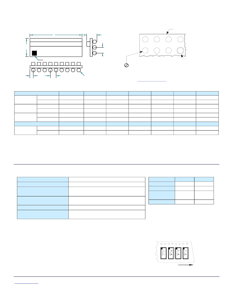
Mechanical Diagrams
K
1.27mm Pitch
L
W
H
P
D
K
Coplanarity
0.15
.006
0.15
.006
0.15
.006
Coplanarity
0.15
.006
mm
inch
mm
inch
mm
inch
11.43
±
0.15
.450
±
.006
11.43
±
0.15
.450
±
.006
11.43
±
0.15
.450
±
.006
L
9.64
±
0.15
.380
±
.006
3.81
±
0.15
.150
±
.006
5.08
±
0.15
.200
±
.006
3.81
±
0.15
.150
±
.006
W
3.64
±
0.15
.143
±
.006
2.03 max
.080 max
2.03 max
.080 max
2.03 max
.080 max
H
1.83 max
.072 max
1.27
±
0.25
.050
±
.010
1.27
±
0.25
.050
±
.010
1.27
±
0.25
.050
±
.010
P
1.00
±
0.25
.039
±
.010
0.76
±
0.05
.030
±
.002
0.76
±
0.05
.030
±
.002
0.76
±
0.05
.030
±
.002
D
0.64
±
0.05
.025
±
.002
1.02
±
0.25
.043
±
.010
1.02
±
0.25
.040
±
.010
1.02
±
0.25
.040
±
.010
K
0.82
±
0.25
.033
±
.010
RC3002B6
RC3005B6
RC3010B6
RC3007B6
RC3008B6
1.0mm Pitch
mm
inch
RC3002B7
Recommended Land Pattern
1.00mm Pitch (B7) = 0.51mm/.020 inch (minimum)
1.27mm pitch (B6) = 0.64mm/.025 inch (minimum)
Outline of Substrate
PCB Pad Diameter
For .006" Thick Solder Paste Stencil, Aperture Opening Should
be Equal to the PCB Pad Diameter.
Refer to
www.ctscorp.com/resistor
for Land Pattern Library
Solder Mask Dia = Pad
Diameter +.15mm
(.006 inch)
RC3___B_ CTSDATE
H
P
P
W
L
(Pitch)
D
A1 Identifier
相關PDF資料 |
PDF描述 |
|---|---|
| RC3005B6TR13 | RC NETWORK, ISOLATED, 1W, 50ohm, 0.1uF, SURFACE MOUNT, 36 |
| RC3007B6TR13 | RC NETWORK, ISOLATED, 1W, 50ohm, 0.0001uF, SURFACE MOUNT, 27 |
| RC3002B6TR7 | RC NETWORK, BUSSED, 1W, 50ohm, 0.1uF, SURFACE MOUNT, 27 |
| RC3002B7TR13 | RC NETWORK, BUSSED, 1W, 50ohm, 0.1uF, SURFACE MOUNT, 27 |
| RC3002B7TR7 | RC NETWORK, BUSSED, 1W, 50ohm, 0.1uF, SURFACE MOUNT, 27 |
相關代理商/技術參數 |
參數描述 |
|---|---|
| RC3007B6 | 制造商:CTS Corporation 功能描述:Cap RC Network 100pF 10% 50 Ohm 1% 1/20W 9R/9C 85 |
| RC3007B6TR13 | 制造商:CTS Corporation 功能描述:RESISTOR RC3007B6TR13 (52 UP) - Tape and Reel |
| RC3007B6TR7 | 制造商:CTS Corporation 功能描述:RESISTOR/CAPACITOR BGA TERMINATOR - Tape and Reel |
| RC3008B6 | 制造商:CTS 制造商全稱:CTS Corporation 功能描述:Integrated Resistor and Capacitor Network RC Series 3000 |
| RC3008B6TR13 | 制造商:CTS Corporation 功能描述:- Tape and Reel |
發(fā)布緊急采購,3分鐘左右您將得到回復。