- 您現(xiàn)在的位置:買賣IC網(wǎng) > PDF目錄373225 > R29773 PDF資料下載
參數(shù)資料
| 型號: | R29773 |
| 文件頁數(shù): | 3/29頁 |
| 文件大小: | 188K |
| 代理商: | R29773 |
第1頁第2頁當前第3頁第4頁第5頁第6頁第7頁第8頁第9頁第10頁第11頁第12頁第13頁第14頁第15頁第16頁第17頁第18頁第19頁第20頁第21頁第22頁第23頁第24頁第25頁第26頁第27頁第28頁第29頁
R296XX/R297XX
PRODUCT SPECIFICATION
2
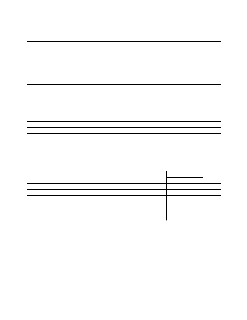
Absolute Maximum Ratings
(above which the useful life may be impaired)
Operating Conditions
Note:
1. Tests shall be conducted at input test conditions as follows: V
IH
= V
IH
(min) +20%, –0%; V
IL
= V
IL
(max) +0%, –50%. Devices
may be tested using any input voltage within this input voltage range but shall be guaranteed to V
IH
(min) and V
IL
(max).
CAUTION: To avoid test correlation problems, the test system noise (e.g., testers, handlers, etc.) should be verified to assure
that V
IH
(min) and V
IL
(max) requirements are not violated at the device terminals.
2. V
IL
= 0.6V for Chip Select Pins on all 29600 series devices.
Supply Voltage to Ground Potential (continuous), V
CC
DC Input Current
DC Input Voltage (address inputs)
DC Input Voltage (chip/power select input pin)
R296XX
R297XX
DC Voltage Applied to Outputs (except during programming)
Output Current into Outputs During Programming
DC Voltage Applied to Outputs During Programming
R296XX
R297XX
Junction Temperature
Storage Temperature
Programming Temperature
Lead Temperature (soldering, 10 seconds)
Current Density (metallization)
Thermal Resistance, Junction-to-Case
q
JC
Dual-ln-Line
Leadless Chip Carrier
Flat Pack
–0.5V to +7.0V
–30 mA to +5.0 mA
–0.5V to +5.5V
–0.5V to +33V
–0.5V to +28V
–0.5V to +V
CC
max.
240 mA
26V
24V
+175
°
C
–65
°
C to +150
°
C
25
±
5
°
C
300
°
C
<5 x 10
5
A/cm
2
£
11
°
C/W
£
10
°
C/W
£
10
°
C/W
Military
Min.
4.5
–55
Parameter
V
CC
T
C
V
IL11, 2
V
IH1
V
IL
V
IH
Description
Supply Voltage
Case Operating Temperature
DC Low Level Input Voltage
DC High Level Input Voltage
AC/Functional Low Level Input Voltage
AC/Functional High Level Input Voltage
Max.
5.5
+125
0.8
Unit
V
°
C
V
V
V
V
2.0
0
3.0
相關(guān)PDF資料 |
PDF描述 |
|---|---|
| R29791 | |
| R29793 | |
| R29771LM | x8 PROM |
| R29773DM | x8 PROM |
| R29773DMS | x8 PROM |
相關(guān)代理商/技術(shù)參數(shù) |
參數(shù)描述 |
|---|---|
| R29773DM | 制造商:未知廠家 制造商全稱:未知廠家 功能描述:x8 PROM |
| R29773DMS | 制造商:未知廠家 制造商全稱:未知廠家 功能描述:x8 PROM |
| R29773FM | 制造商:未知廠家 制造商全稱:未知廠家 功能描述:x8 PROM |
| R29773FM/883B | 制造商:未知廠家 制造商全稱:未知廠家 功能描述:x8 PROM |
| R29773FMS | 制造商:未知廠家 制造商全稱:未知廠家 功能描述:x8 PROM |
發(fā)布緊急采購,3分鐘左右您將得到回復(fù)。