- 您現(xiàn)在的位置:買賣IC網(wǎng) > PDF目錄299802 > QS5V991-2JRC (INTEGRATED DEVICE TECHNOLOGY INC) QS5 SERIES, PLL BASED CLOCK DRIVER, 8 TRUE OUTPUT(S), 0 INVERTED OUTPUT(S), PQCC32 PDF資料下載
參數(shù)資料
| 型號: | QS5V991-2JRC |
| 廠商: | INTEGRATED DEVICE TECHNOLOGY INC |
| 元件分類: | 時鐘及定時 |
| 英文描述: | QS5 SERIES, PLL BASED CLOCK DRIVER, 8 TRUE OUTPUT(S), 0 INVERTED OUTPUT(S), PQCC32 |
| 封裝: | PLASTIC, LCC-32 |
| 文件頁數(shù): | 3/8頁 |
| 文件大?。?/td> | 158K |
| 代理商: | QS5V991-2JRC |
3
COMMERCIALANDINDUSTRIALTEMPERATURERANGES
QS5V991
3.3V PROGRAMMABLE SKEW PLL CLOCK DRIVER TURBOCLOCK
EXTERNALFEEDBACK
By providing external feedback, the QS5V991 gives users flexibility
with regard to skew adjustment. The FB signal is compared with the
input REF signal at the phase detector in order to drive the VCO. Phase
differences cause the VCO of the PLL to adjust upwards or downwards
accordingly.
NOTES:
1. The device may be operated outside recommended frequency ranges without damage, but functional operation is not guaranteed. Selecting the ap-
propriate FS value based on input frequency range allows the PLL to operate in its ‘sweet spot’ where jitter is lowest.
2. The level to be set on FS is determined by the nominal operating frequency of the VCO and Time Unit Generator. The VCO frequency always ap-
pears at 1Q1:0, 2Q1:0, and the higher outputs when they are operated in their undivided modes. The frequency appearing at the REF and FB inputs will
be the same as the VCO when the output connected to FB is undivided. The frequency of the REF and FB inputs will be 1/2 or 1/4 the VCO frequency
when the part is configured for a frequency multiplication by using a divided output as the FB input.
3. Skew adjustment range assumes that a zero skew output is used for feedback. If a skewed Q output is used for feedback, then adjustment range will
be greater. For example if a 4tU skewed output is used for feedback, all other outputs will be skewed –4tU in addition to whatever skew value is programmed
for those outputs. ‘Max adjustment’ range applies to output pairs 3 and 4 where ± 6tU skew adjustment is possible and at the lowest FNOM value.
4. The maximum REF Clock Input Frequency is 70MHz. Use Q/2 or Q/4 as feedback and use the Control Summary Table explicitly for output frequency
to 85MHz.
An internal loop filter moderates the response of the VCO to the
phase detector. The loop filter transfer function has been chosen to
provide minimal jitter (or frequency variation) while still providing accu-
rate responses to input frequency changes.
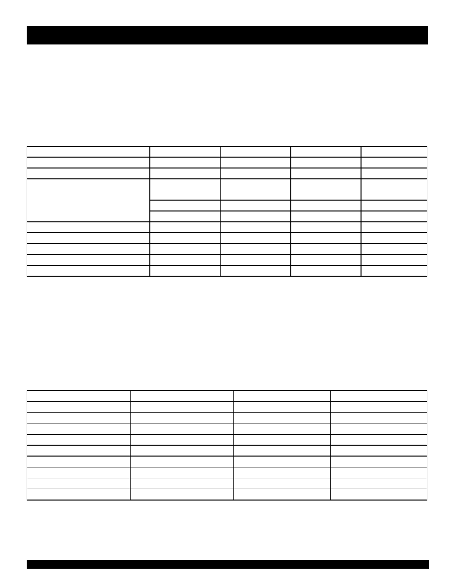
CONTROL SUMMARY TABLE FOR FEEDBACK SIGNALS
nF1:0
Skew (Pair #1, #2)
Skew (Pair #3)
Skew (Pair #4)
LL (1)
–4tU
Divide by 2
LM
–3tU
–6tU
LH
–2tU
–4tU
ML
–1tU
–2tU
MM
Zero Skew
MH
1tU
2tU
HL
2tU
4tU
HM
3tU
6tU
HH
4tU
Divide by 4
Inverted (2)
NOTES:
1.
LL disables outputs if TEST = MID and GND/
sOE = HIGH.
2.
When pair #4 is set to HH (inverted), GND/
sOE disables pair #4 HIGH when VCCQ/PE = HIGH, GND/ sOE disables pair #4 LOW when VCCQ/PE =
LOW.
PLL PROGRAMMABLE SKEW RANGE AND RESOLUTION TABLE
FS = LOW
FS = MID
FS = HIGH
Comments
Timing Unit Calculation (tU)
1/(44 x FNOM)
1/(26 x FNOM)
1/(16 x FNOM)
VCO Frequency Range (FNOM) (1,2)
25 to 35MHz
35 to 60MHz
60 to 85 MHz
Skew Adjustment Range (3)
Max Adjustment:
±9.09ns
±9.23ns
±9.38ns
ns
±49
±83
±135
Phase Degrees
±14%
±23%
±37%
% of Cycle Time
Example 1, FNOM = 25MHz
tU = 0.91ns
—
Example 2, FNOM = 30MHz
tU = 0.76ns
—
Example 3, FNOM = 40MHz
—
tU = 0.96ns
—
Example 4, FNOM = 50MHz
—
tU = 0.77ns
—
Example 5, FNOM = 80MHz
—
tU = 0.78ns
相關(guān)PDF資料 |
PDF描述 |
|---|---|
| QS74FCT162244ATQ1 | FCT SERIES, QUAD 4-BIT DRIVER, TRUE OUTPUT, PDSO48 |
| QS74FCT162373CTPV | FCT SERIES, DUAL 8-BIT DRIVER, TRUE OUTPUT, PDSO48 |
| QS74FCT16841CTPA | FCT SERIES, DUAL 10-BIT DRIVER, TRUE OUTPUT, PDSO56 |
| QS74FCT2374CTS1 | FCT SERIES, 8-BIT DRIVER, TRUE OUTPUT, PDSO20 |
| QS74FCT2374TQB | FCT SERIES, 8-BIT DRIVER, TRUE OUTPUT, PDSO20 |
相關(guān)代理商/技術(shù)參數(shù) |
參數(shù)描述 |
|---|---|
| QS5V991-7JR1 | 制造商:QSI 功能描述: |
| QS5V99320QC | 制造商:QUALITY 功能描述:QS5V993-2QC |
| QS5W1 | 制造商:ROHM 制造商全稱:Rohm 功能描述:Midium Power Transistors (30V / 3A) |
| QS5W2 | 制造商:ROHM 制造商全稱:Rohm 功能描述:Midium Power Transistors (50V / 3A) |
| QS5W2TR | 制造商:ROHM Semiconductor 功能描述: |
發(fā)布緊急采購,3分鐘左右您將得到回復(fù)。