- 您現(xiàn)在的位置:買賣IC網(wǎng) > PDF目錄98066 > PWR-82520-300 (DATA DEVICE CORP) BRUSHLESS DC MOTOR CONTROLLER, 15 A, DIP41 PDF資料下載
參數(shù)資料
| 型號: | PWR-82520-300 |
| 廠商: | DATA DEVICE CORP |
| 元件分類: | 運動控制電子 |
| 英文描述: | BRUSHLESS DC MOTOR CONTROLLER, 15 A, DIP41 |
| 封裝: | DIP-41 |
| 文件頁數(shù): | 6/12頁 |
| 文件大?。?/td> | 174K |
| 代理商: | PWR-82520-300 |
3
INTRODUCTION
The PWR-82520 is high performance current control (torque
loop) hybrid which use complementary four quadrant switching
topology (See BASIC OPERATION) to provide linearity through
zero current. The high Pulse Width Modulation (PWM) switching
frequency makes it suitable for even low inductance motors. The
PWR-82520 hybrid can accept single-ended or differential mode
command signals. The current gain can be easily programmed
to match the end user system requirements. With the compen-
sation network externally wired, the hybrid can provide optimum
control of a wide range of loads.
The PWR-82520 uses unique current sense technology and a
non-inductive hybrid sense resistor which yields a highly linear
current output over the wide military temperature range (see
FIGURE 9). The output current non-linearity is better than 3%
over the operating temperature range and the total error due to
all the factors such as offset, initial component accuracies etc. is
maintained well below 5% of the rated output current.
The Hall sensor interface for current commutation has built-in
decoder logic that separates illegal codes and ensures that there
is no cross conduction. The hybrid also has a +15V supply out-
put for powering the Hall sensors. The Hall sensor inputs are
internally pulled up to +5V and they can be driven from open-col-
lector outputs.
The PWM frequency can be programmed externally by adding a
capacitor from PWM OUT to PWM GND. In addition, multiple
PWR-82520’s can be synchronized by using one device as a
master and connecting its PWM OUT pin to the PWM IN of all
the other slave devices in a system or by applying a SYNC pulse
to pin 22.
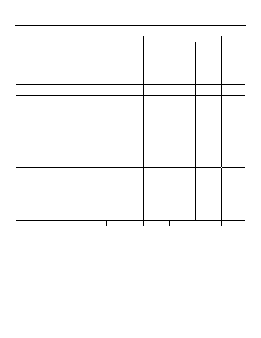
TABLE 2. PWR-82520 SPECIFICATIONS (CONTINUED)
(Unless otherwise specified, VBUS = 28 VDC, V
DD = +15V, VEE = -15V, TC = 25°C)
PARAMETERS
SYMBOL
TEST CONDITIONS
VALUE
UNITS
MIN
TYP
MAX
PWM IN
+Peak
-Peak
Frequency
Non -linearity
Duty Cycle
V
P+
V
P-
f
LIN
D CYCLE
9.8
-10.2
10
-2
49
10.0
-10.0
50
10.2
-9.8
60
+2
51
V
KHz
%
PWM OUT
Free Run Frequency
45
50
55
KHz
HALL POWER SUPPLY
Max Current Draw
I
MDRW
50
mA
HALL SIGNALS
Logic 1
Logic 0
HA, HB,
HC
3.5
—
0.7
VDC
ENABLE INPUT
Enabled
Disabled
ENABLE
—
3.5
0.7
—
VDC
ISOLATION
CASE to PIN
500 VDC HIPOT
10
M
THERMAL
Thermal Resistance
Junction - Case
Case - Air
Junction Temperature
Case Operating Temperature
Case Storage Temperature
PROPAGATION DELAY
SWITCHING CHARACTERISTICS
Upper drive
Turn-on Rise Time
Turn-off Fall Time
Lower drive
Turn-on Rise Time
Turn-off Fall Time
Diode Forward Voltage Drop
θ
J-C
θ
C-A
T
J
T
C
T
CS
Td (on)
Td (off)
tr
tf
tr
tf
VF
Ip = 4A
From 0.7V on ENABLE
to 10% of VOUT
From 3.5V on ENABLE
to 90% of VOUT
Ip =4 A
ID = 1A
-55
-65
6
10
+175
+125
+150
40
20
125
200
1.25
°C/W
°C
s
ns
V
WEIGHT
1.7(48)
oz(gr)
相關(guān)PDF資料 |
PDF描述 |
|---|---|
| PWR-82520-200 | BRUSHLESS DC MOTOR CONTROLLER, 15 A, DIP41 |
| PWR-82520-800 | BRUSHLESS DC MOTOR CONTROLLER, 15 A, DIP41 |
| PWR-82520-100 | BRUSHLESS DC MOTOR CONTROLLER, 15 A, DIP41 |
| PWR-82520-400 | BRUSHLESS DC MOTOR CONTROLLER, 15 A, DIP41 |
| PWR-SMP211BNI | 8 A SWITCHING CONTROLLER, 272 kHz SWITCHING FREQ-MAX, PDIP16 |
相關(guān)代理商/技術(shù)參數(shù) |
參數(shù)描述 |
|---|---|
| PWR-82520-300K | 制造商:未知廠家 制造商全稱:未知廠家 功能描述:Industrial Control IC |
| PWR-82520-300L | 制造商:未知廠家 制造商全稱:未知廠家 功能描述:Industrial Control IC |
| PWR-82520-300Q | 制造商:未知廠家 制造商全稱:未知廠家 功能描述:Industrial Control IC |
| PWR-82520-300S | 制造商:未知廠家 制造商全稱:未知廠家 功能描述:Industrial Control IC |
| PWR-82520-300W | 制造商:未知廠家 制造商全稱:未知廠家 功能描述:Industrial Control IC |
發(fā)布緊急采購,3分鐘左右您將得到回復。