- 您現(xiàn)在的位置:買(mǎi)賣(mài)IC網(wǎng) > PDF目錄98062 > PT6341C (TEXAS INSTRUMENTS INC) 6 A SWITCHING REGULATOR, 400 kHz SWITCHING FREQ-MAX, SMA12 PDF資料下載
參數(shù)資料
| 型號(hào): | PT6341C |
| 廠商: | TEXAS INSTRUMENTS INC |
| 元件分類(lèi): | 穩(wěn)壓器 |
| 英文描述: | 6 A SWITCHING REGULATOR, 400 kHz SWITCHING FREQ-MAX, SMA12 |
| 封裝: | SMD-12 |
| 文件頁(yè)數(shù): | 4/11頁(yè) |
| 文件大小: | 199K |
| 代理商: | PT6341C |
For technical support and more information, see inside back cover or visit www.ti.com
PT6340 Series
6-A 12-V Input Adjustable
Integrated Switching Regulator
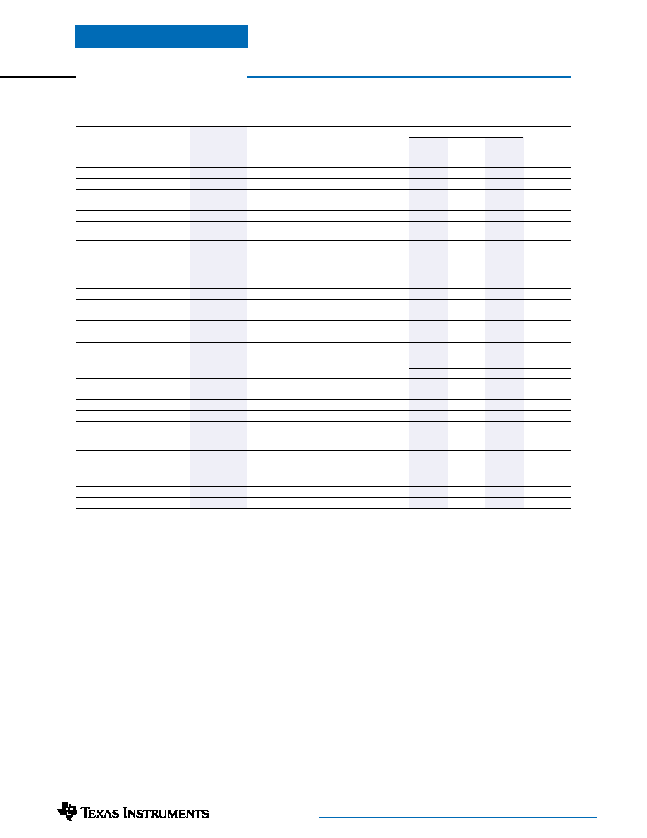
Specifications (Unless otherwise stated, Ta =25°C, Vin =12V, Cin =100F, Cout =330F, and Io =Iomax)
PT6340 SERIES
Characteristic
Symbol
Conditions
Min
Typ
Max
Units
Output Current
Io
Ta =+60°C, 200LFM
0.1 (1)
—6
A
Ta =+25°C, natural convection
0.1 (1)
—6
Input Voltage Range
Vin
Over Io Range
10.8
—
13.2
VDC
Set Point Voltage Tolerance
Vo tol
—
±1±2%Vo
Temperature Variation
Regtemp
–40°
≤Ta≤ +85°C, Io =Iomin
—
±0.5
—
%Vo
Line Regulation
Regline
Over Vin range
—
±5
±10
mV
Load Regulation
Regload
Over Io range
—
±5
±15
mV
Total Output Voltage Variation
Votot
Includes set-point, line, load,
—
±2±3%Vo
–40°
≤Ta ≤ +85°C
Efficiency
η
Io =4A
Vo =5.0V
—
93
—
Vo =3.3V
—
92
—
Vo =2.5V
—
91
—
%
Vo =1.8V
—
89
—
Vo =1.5V
—
87
—
Vo =1.2V
—
85
—
Vo Ripple (pk-pk)
Vr
20MHz bandwidth
—
20
—
mVpp
Transient Response
ttr
1A/s load step, 50% to 100% Iomax—
50
—
s
Vtr
Vo over/undershoot
—
±60
—
mV
Short Circuit Threshold
Isc threshold
—
8.5
—
A
Switching Frequency
s
Over Vin and Io range
300
350
400
kHz
Inhibit (Pin 1)
Referenced to GND (pin 5)
High-Level Input Voltage
VIH
Vin–0.5
—
Open (2)
V
Low-Level Input Voltage
VIL
–0.2
—
+0.5
Low-Level Input Current
IIL
—
–0.5
–
mA
Standby Input Current
Iin standby
pins 1 & 5 connected
—
+0.5
—
mA
External Output Capacitance
Cout
See application schematic
330
—
1,000
F
External Input Capacitance
Cin
See application schematic
100
—
F
Operating Temperature Range
Ta
Over Vin range
–40 (3)
—
+85 (4)
°C
Storage Temperature
Ts
—
–40
—
+125
°C
Reliability
MTBF
Per Bellcore TR-332
8.8
—
106 Hrs
50% stress, Ta =40°C, ground benign
Mechanical Shock
—
Per Mil-Std-883D, method 2002.3,
—
500
—
G’s
1ms, half-sine, mounted to a fixture
Mechanical Vibration
—
Mil-Std-883D, Method 2007.2,
—
20 (5)
—
G’s
20-2000Hz, soldered in PCB
Weight
—
23
—
grams
Flammability
—
Materials meet UL 94V-0
Notes:
(1) The ISR will operate at no load with reduced specifications.
(2) The Inhibit control (pin 1) has an internal pull-up and if it is left open circuit the module will operate when input power is applied. The open-circuit
voltage is the input voltage Vin. Use a discrete MOSFET to control the Inhibit pin, and ensure a transitioin time of less than ≤10s. Consult the related
application note for other interface considerations.
(3) For operation below 0°C, Cin and Cout must have stable characteristics. Use either low ESR tantalum or Oscon capacitors.
(4) See Safe Operating Area curves or contact the factory for the appropriate derating.
(5) The case pins on through-hole package types (suffixes N & A) must be soldered. For more information consult the applicable package outline drawing.
Input/Output Capacitors:
The PT6340 regulator series requires a 100F electrolytic (or tantalum) capacitor at the input and 330F at the output for proper
operation in all applications. In addition, the input capacitance, Cin, must be rated for a minimum of 740mArms of ripple current, and the ESR of the output
capacitor, Cout, must less than 50m @100kHz. For transient or dynamic load applications additional output capacitance may be necessary. For more information
consult the related application note on capacitor recommendations.
相關(guān)PDF資料 |
PDF描述 |
|---|---|
| PT6365N | 11 A SWITCHING REGULATOR, 400 kHz SWITCHING FREQ-MAX, MSMA18 |
| PT6367C | 11 A SWITCHING REGULATOR, 400 kHz SWITCHING FREQ-MAX, MSMA18 |
| PT6364C | 11 A SWITCHING REGULATOR, 400 kHz SWITCHING FREQ-MAX, MSMA18 |
| PT6367N | 11 A SWITCHING REGULATOR, 400 kHz SWITCHING FREQ-MAX, MSMA18 |
| PT6366N | 11 A SWITCHING REGULATOR, 400 kHz SWITCHING FREQ-MAX, MSMA18 |
相關(guān)代理商/技術(shù)參數(shù) |
參數(shù)描述 |
|---|---|
| PT6341N | 功能描述:DC/DC轉(zhuǎn)換器 5Vout 6A 12V-Input Adj Step-Down ISR RoHS:否 制造商:Murata 產(chǎn)品: 輸出功率: 輸入電壓范圍:3.6 V to 5.5 V 輸入電壓(標(biāo)稱(chēng)): 輸出端數(shù)量:1 輸出電壓(通道 1):3.3 V 輸出電流(通道 1):600 mA 輸出電壓(通道 2): 輸出電流(通道 2): 安裝風(fēng)格:SMD/SMT 封裝 / 箱體尺寸: |
| PT6342 | 制造商:TI 制造商全稱(chēng):Texas Instruments 功能描述:6-A 12-V Input Adjustable Integrated Switching Regulator |
| PT6342A | 功能描述:DC/DC轉(zhuǎn)換器 3.3Vout 6A 12V-Input Adj Step-Down ISR RoHS:否 制造商:Murata 產(chǎn)品: 輸出功率: 輸入電壓范圍:3.6 V to 5.5 V 輸入電壓(標(biāo)稱(chēng)): 輸出端數(shù)量:1 輸出電壓(通道 1):3.3 V 輸出電流(通道 1):600 mA 輸出電壓(通道 2): 輸出電流(通道 2): 安裝風(fēng)格:SMD/SMT 封裝 / 箱體尺寸: |
| PT6342A2 | 制造商:Rochester Electronics LLC 功能描述:- Bulk |
| PT6342C | 功能描述:DC/DC轉(zhuǎn)換器 3.3Vout 6A 12V-Input Adj Step-Down ISR RoHS:否 制造商:Murata 產(chǎn)品: 輸出功率: 輸入電壓范圍:3.6 V to 5.5 V 輸入電壓(標(biāo)稱(chēng)): 輸出端數(shù)量:1 輸出電壓(通道 1):3.3 V 輸出電流(通道 1):600 mA 輸出電壓(通道 2): 輸出電流(通道 2): 安裝風(fēng)格:SMD/SMT 封裝 / 箱體尺寸: |
發(fā)布緊急采購(gòu),3分鐘左右您將得到回復(fù)。