- 您現(xiàn)在的位置:買賣IC網(wǎng) > PDF目錄296863 > PSD835F1V-12B81I (意法半導(dǎo)體) Configurable Memory System on a Chip for 8-Bit Microcontrollers PDF資料下載
參數(shù)資料
| 型號: | PSD835F1V-12B81I |
| 廠商: | 意法半導(dǎo)體 |
| 英文描述: | Configurable Memory System on a Chip for 8-Bit Microcontrollers |
| 中文描述: | 在8片位微控制器可配置存儲系統(tǒng) |
| 文件頁數(shù): | 44/110頁 |
| 文件大小: | 570K |
| 代理商: | PSD835F1V-12B81I |
第1頁第2頁第3頁第4頁第5頁第6頁第7頁第8頁第9頁第10頁第11頁第12頁第13頁第14頁第15頁第16頁第17頁第18頁第19頁第20頁第21頁第22頁第23頁第24頁第25頁第26頁第27頁第28頁第29頁第30頁第31頁第32頁第33頁第34頁第35頁第36頁第37頁第38頁第39頁第40頁第41頁第42頁第43頁當(dāng)前第44頁第45頁第46頁第47頁第48頁第49頁第50頁第51頁第52頁第53頁第54頁第55頁第56頁第57頁第58頁第59頁第60頁第61頁第62頁第63頁第64頁第65頁第66頁第67頁第68頁第69頁第70頁第71頁第72頁第73頁第74頁第75頁第76頁第77頁第78頁第79頁第80頁第81頁第82頁第83頁第84頁第85頁第86頁第87頁第88頁第89頁第90頁第91頁第92頁第93頁第94頁第95頁第96頁第97頁第98頁第99頁第100頁第101頁第102頁第103頁第104頁第105頁第106頁第107頁第108頁第109頁第110頁
PSD8XX Family
PSD835G2
38
The
PSD835G2
Functional
Blocks
(cont.)
9.2.2.1 Output Micro
Cell
Eight of the Output Micro
Cells are connected to Port A pins are named as McellA0-7.
The other eight Micro
Cells are connected to Port B pins are named as McellB0-7.
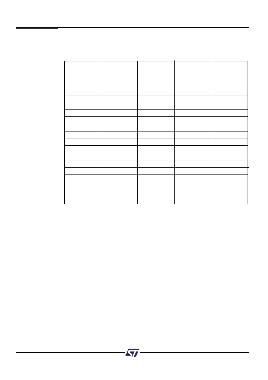
Maximum
Native
Borrowed
Data Bit for
Output
Port
Product
Loading or
Micro
Cell
Assignment
Terms
Reading
McellA0
Port A0
3
6
D0
McellA1
Port A1
3
6
D1
McellA2
Port A2
3
6
D2
McellA3
Port A3
3
6
D3
McellA4
Port A4
3
6
D4
McellA5
Port A5
3
6
D5
McellA6
Port A6
3
6
D6
McellA7
Port A7
3
6
D7
McellB0
Port B0
4
5
D0
McellB1
Port B1
4
5
D1
McellB2
Port B2
4
5
D2
McellB3
Port B3
4
5
D3
McellB4
Port B4
4
6
D4
McellB5
Port B5
4
6
D5
McellB6
Port B6
4
6
D6
McellB7
Port B7
4
6
D7
Table 13. Output Micro
Cell Port and Data Bit Assignments
The Output Micro
Cell (OMC) architecture is shown in Figure 13. As shown in the figure,
there are native product terms available from the AND array, and borrowed product terms
available (if unused) from other OMCs. The polarity of the product term is controlled by the
XOR gate. The OMC can implement either sequential logic, using the flip-flop element, or
combinatorial logic. The multiplexer selects between the sequential or combinatorial logic
outputs. The multiplexer output can drive a Port pin and has a feedback path to the AND
array inputs.
The flip-flop in the OMC can be configured as a D, T, JK, or SR type in the PSDsoft
program. The flip-flop’s clock, preset, and clear inputs may be driven from a product term
of the AND array. Alternatively, the external CLKIN signal can be used for the clock input
to the flip-flop. The flip-flop is clocked on the rising edge of the clock input. The preset and
clear are active-high inputs. Each clear input can use up to two product terms.
相關(guān)PDF資料 |
PDF描述 |
|---|---|
| PSD835F1V-12J | CONN RECEPT 26POS 2MM IDT GOLD |
| PSD835F1V-12JI | Configurable Memory System on a Chip for 8-Bit Microcontrollers |
| PSD835F1V-12M | Configurable Memory System on a Chip for 8-Bit Microcontrollers |
| PSD835F2V-12B81I | Configurable Memory System on a Chip for 8-Bit Microcontrollers |
| PSD913F1V-12B81 | Flash In-System Programmable ISP Peripherals For 8-bit MCUs |
相關(guān)代理商/技術(shù)參數(shù) |
參數(shù)描述 |
|---|---|
| PSD835G2-70U | 功能描述:靜態(tài)隨機存取存儲器 5.0V 4M 70ns RoHS:否 制造商:Cypress Semiconductor 存儲容量:16 Mbit 組織:1 M x 16 訪問時間:55 ns 電源電壓-最大:3.6 V 電源電壓-最小:2.2 V 最大工作電流:22 uA 最大工作溫度:+ 85 C 最小工作溫度:- 40 C 安裝風(fēng)格:SMD/SMT 封裝 / 箱體:TSOP-48 封裝:Tray |
| PSD835G2-90U | 功能描述:靜態(tài)隨機存取存儲器 5.0V 4M 90ns RoHS:否 制造商:Cypress Semiconductor 存儲容量:16 Mbit 組織:1 M x 16 訪問時間:55 ns 電源電壓-最大:3.6 V 電源電壓-最小:2.2 V 最大工作電流:22 uA 最大工作溫度:+ 85 C 最小工作溫度:- 40 C 安裝風(fēng)格:SMD/SMT 封裝 / 箱體:TSOP-48 封裝:Tray |
| PSD835G2-90UI | 功能描述:靜態(tài)隨機存取存儲器 5.0V 4M 90ns RoHS:否 制造商:Cypress Semiconductor 存儲容量:16 Mbit 組織:1 M x 16 訪問時間:55 ns 電源電壓-最大:3.6 V 電源電壓-最小:2.2 V 最大工作電流:22 uA 最大工作溫度:+ 85 C 最小工作溫度:- 40 C 安裝風(fēng)格:SMD/SMT 封裝 / 箱體:TSOP-48 封裝:Tray |
| PSD835G2V-12UI | 功能描述:靜態(tài)隨機存取存儲器 3.0V 4M 120ns RoHS:否 制造商:Cypress Semiconductor 存儲容量:16 Mbit 組織:1 M x 16 訪問時間:55 ns 電源電壓-最大:3.6 V 電源電壓-最小:2.2 V 最大工作電流:22 uA 最大工作溫度:+ 85 C 最小工作溫度:- 40 C 安裝風(fēng)格:SMD/SMT 封裝 / 箱體:TSOP-48 封裝:Tray |
| PSD835G2V-90U | 功能描述:靜態(tài)隨機存取存儲器 3.0V 4M 90ns RoHS:否 制造商:Cypress Semiconductor 存儲容量:16 Mbit 組織:1 M x 16 訪問時間:55 ns 電源電壓-最大:3.6 V 電源電壓-最小:2.2 V 最大工作電流:22 uA 最大工作溫度:+ 85 C 最小工作溫度:- 40 C 安裝風(fēng)格:SMD/SMT 封裝 / 箱體:TSOP-48 封裝:Tray |
發(fā)布緊急采購,3分鐘左右您將得到回復(fù)。