- 您現(xiàn)在的位置:買賣IC網(wǎng) > PDF目錄224800 > PSD4235G2V-B-90B81I (意法半導體) Flash In-System-Programmable Peripherals for 16-Bit MCUs PDF資料下載
參數(shù)資料
| 型號: | PSD4235G2V-B-90B81I |
| 廠商: | 意法半導體 |
| 英文描述: | Flash In-System-Programmable Peripherals for 16-Bit MCUs |
| 中文描述: | Flash在系統(tǒng)可編程外設(shè)的16位微控制器 |
| 文件頁數(shù): | 58/93頁 |
| 文件大?。?/td> | 503K |
| 代理商: | PSD4235G2V-B-90B81I |
第1頁第2頁第3頁第4頁第5頁第6頁第7頁第8頁第9頁第10頁第11頁第12頁第13頁第14頁第15頁第16頁第17頁第18頁第19頁第20頁第21頁第22頁第23頁第24頁第25頁第26頁第27頁第28頁第29頁第30頁第31頁第32頁第33頁第34頁第35頁第36頁第37頁第38頁第39頁第40頁第41頁第42頁第43頁第44頁第45頁第46頁第47頁第48頁第49頁第50頁第51頁第52頁第53頁第54頁第55頁第56頁第57頁當前第58頁第59頁第60頁第61頁第62頁第63頁第64頁第65頁第66頁第67頁第68頁第69頁第70頁第71頁第72頁第73頁第74頁第75頁第76頁第77頁第78頁第79頁第80頁第81頁第82頁第83頁第84頁第85頁第86頁第87頁第88頁第89頁第90頁第91頁第92頁第93頁
PSD4000 Series
Preliminary Information
58
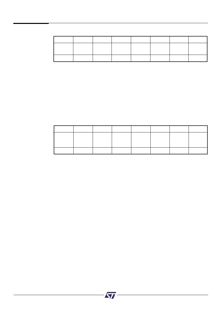
Bit 1 0 = Automatic Power Down (APD) is disabled.
1 = Automatic Power Down (APD) is enabled.
Bit 3 0 = PLD Turbo is on.
1 = PLD Turbo is off, saving power.
Bit 4 0 = CLKIN input to the PLD AND array is connected.
Every CLKIN change will power up the PLD when Turbo bit is off.
1 = CLKIN input to PLD AND array is disconnected, saving power.
Bit 7
Bit 6
Bit 5
Bit 4
Bit 3
Bit 2
Bit 1
Bit 0
**
*
PLD
*
APD
*
Array clk
Turbo
Enable
1 = off
1 = on
Table 26. Power Management Mode Registers (PMMR0, PMMR2)**
PMMR0
***Bits 0, 2, 6, and 7 are not used, and should be set to 0, bit 5 should be set to 1.
***The PMMR0, and PMMR2 register bits are cleared to zero following power up.
***Subsequent reset pulses will not clear the registers.
The
PSD4000
Functional
Blocks
(cont.)
Bit 7
Bit 6
Bit 5
Bit 4
Bit 3
Bit 2
Bit 1
Bit 0
*
PLD
**
PLD
**
PLD
**
*
PLD
array
WRH/DBE
ALE
CNTL2
CNTL1
CNTL0
Addr.
1 = off
PMMR2
Bit 0 0 = Address A[7:0] inputs to the PLD AND array are connected.
1 = Address A[7:0] inputs to the PLD AND array are disconnected, saving power.
Note: In 80C51XA mode, A[7:1] comes from Port F (PF1-PF3) and AD10 [3:0].
Bit 2 0 = Cntl0 input to the PLD AND array is connected.
1 = Cntl0 input to PLD AND array is disconnected, saving power.
Bit 3 0 = Cntl1 input to the PLD AND array is connected.
1 = Cntl1 input to PLD AND array is disconnected, saving power.
Bit 4 0 = Cntl2 input to the PLD AND array is connected.
1 = Cntl2 input to PLD AND array is disconnected, saving power.
Bit 5 0 = ALE input to the PLD AND array is connected.
1 = ALE input to PLD AND array is disconnected, saving power.
Bit 6 0 = WRH/DBE input to the PLD AND array is connected.
1 = WRH/DBE input to PLD AND array is disconnected, saving power.
**Unused bits should be set to 0.
**Refer to Table 14 the signals that are blocked on pins CNTL0-2.
發(fā)布緊急采購,3分鐘左右您將得到回復。