- 您現(xiàn)在的位置:買賣IC網(wǎng) > PDF目錄98060 > PS395CPG (PERICOM SEMICONDUCTOR CORP) OCTAL 1-CHANNEL, SGL POLE SGL THROW SWITCH, PDIP24 PDF資料下載
參數(shù)資料
| 型號(hào): | PS395CPG |
| 廠商: | PERICOM SEMICONDUCTOR CORP |
| 元件分類: | 多路復(fù)用及模擬開關(guān) |
| 英文描述: | OCTAL 1-CHANNEL, SGL POLE SGL THROW SWITCH, PDIP24 |
| 封裝: | PLASTIC, DIP-24 |
| 文件頁(yè)數(shù): | 2/13頁(yè) |
| 文件大?。?/td> | 405K |
| 代理商: | PS395CPG |
第1頁(yè)當(dāng)前第2頁(yè)第3頁(yè)第4頁(yè)第5頁(yè)第6頁(yè)第7頁(yè)第8頁(yè)第9頁(yè)第10頁(yè)第11頁(yè)第12頁(yè)第13頁(yè)
10
PS8462B
01/12/01
12345678901234567890123456789012123456789012345678901234567890121234567890123456789012345678901212345678901234567890123456789012123456789012
PS395
Precision8-Channel17V,
SPSTSwitchw/SerialControl
Detailed Description
Basic Operation
The PS395s interface can be thought of as an 8-bit shift register
controlled by CS (Figure 7). While CS is low, input data appearing
at DIN is clocked into the shift register synchronously with SCLKs
rising edge. The data is an 8-bit word, each bit controlling one of
eight switches in the PS395. DOUT is the shift registers output,
with data appearing synchronously with SCLKs falling edge. Data
at DOUT is simply the input data delayed by eight clock cycles.
When shifting the input data, D7 is the first bit in and out of the
shift register. While shifting data, the switches remain in their pre-
vious configuration. When the eight bits of data have been shifted
in, CS is driven high. This updates the new switch configuration
and inhibits further data from entering the shift register. Transi-
tions at DIN and SCLK have no effect when CS is high, and DOUT
holds the first input bit (D7) at its output.
More or less than eight clock cycles can be entered during the CS
low period. When this happens, the shift register will contain only
the last eight serial data bits, regardless of when they were en-
tered. On the rising edge of CS, all the switches will be set to the
corresponding states.
The PS395s three-wire serial interface is compatible with SPI,
QSPI, and Microwire standards. If inter-facing with a Motorola
processor serial interface, set CPOL = 0. The PS395 is considered a
slave device (Figures 2 and 7). Upon power-up, the shift register
contains all zeros, and all switches are off.
The latch that drives the analog switch is updated on the rising
edge of CS, regardless of SCLKs state. This meets all the SPI and
QSPI requirements.
Daisy Chaining
For a simple interface using several PS395s, daisy chain the shift
registers as shown in Figure 5. The CS pins of all devices are
connected together, and a stream of data is shifted through the
PS395s in series. When CS is brought high, all switches are up-
dated simultaneously. Additional shift registers may be included
anywhere in series with the PS395 data chain.
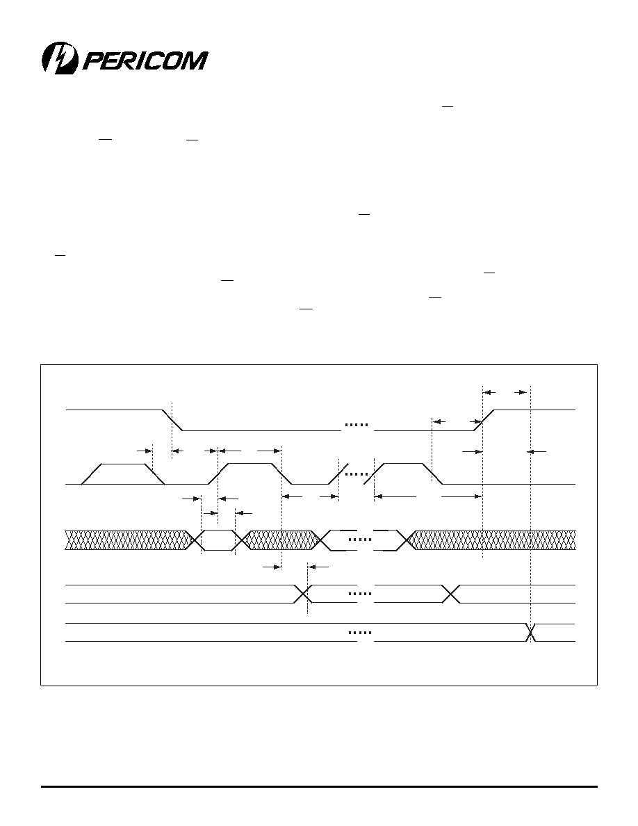
tCSH0
SCLK
DIN
DOUT
COM OUT
tCSS
tCL
tDS
tDH
tDO
tCSH1
tOFF
tCSH2
tCLL
tCH
Figure 1. Timing Diagram
相關(guān)PDF資料 |
PDF描述 |
|---|---|
| PS399EEE | 4-CHANNEL, DIFFERENTIAL MULTIPLEXER, PDSO16 |
| PS398EEE | 8-CHANNEL, SGL ENDED MULTIPLEXER, PDSO16 |
| PS4531CPP | 4-CHANNEL, DIFFERENTIAL MULTIPLEXER, PDIP20 |
| PS4532CPP | TRIPLE 2-CHANNEL, SGL ENDED MULTIPLEXER, PDIP20 |
| PS4532EPP | TRIPLE 2-CHANNEL, SGL ENDED MULTIPLEXER, PDIP20 |
相關(guān)代理商/技術(shù)參數(shù) |
參數(shù)描述 |
|---|---|
| PS395CWG | 制造商:未知廠家 制造商全稱:未知廠家 功能描述:ANALOG SWITCH|OCTAL|SPST|CMOS|SOP|24PIN|PLASTIC |
| PS395ENG | 制造商:未知廠家 制造商全稱:未知廠家 功能描述:ANALOG SWITCH|OCTAL|SPST|CMOS|DIP|24PIN|PLASTIC |
| PS395EWG | 制造商:未知廠家 制造商全稱:未知廠家 功能描述:ANALOG SWITCH|OCTAL|SPST|CMOS|SOP|24PIN|PLASTIC |
| PS396 | 制造商:PERICOM 制造商全稱:Pericom Semiconductor Corporation 功能描述:Precision, 16-Channel 17V Analog Multiplexer |
| PS396CAI | 制造商:PERICOM 制造商全稱:Pericom Semiconductor Corporation 功能描述:Precision, 16-Channel 17V Analog Multiplexer |
發(fā)布緊急采購(gòu),3分鐘左右您將得到回復(fù)。