- 您現(xiàn)在的位置:買賣IC網(wǎng) > PDF目錄98060 > PS395AEWG (PERICOM SEMICONDUCTOR CORP) OCTAL 1-CHANNEL, SGL POLE SGL THROW SWITCH, PDSO24 PDF資料下載
參數(shù)資料
| 型號(hào): | PS395AEWG |
| 廠商: | PERICOM SEMICONDUCTOR CORP |
| 元件分類: | 多路復(fù)用及模擬開(kāi)關(guān) |
| 英文描述: | OCTAL 1-CHANNEL, SGL POLE SGL THROW SWITCH, PDSO24 |
| 封裝: | SOIC-24 |
| 文件頁(yè)數(shù): | 3/13頁(yè) |
| 文件大小: | 405K |
| 代理商: | PS395AEWG |
第1頁(yè)第2頁(yè)當(dāng)前第3頁(yè)第4頁(yè)第5頁(yè)第6頁(yè)第7頁(yè)第8頁(yè)第9頁(yè)第10頁(yè)第11頁(yè)第12頁(yè)第13頁(yè)
11
PS8463C
03/07/01
12345678901234567890123456789012123456789012345678901234567890121234567890123456789012345678901212345678901234567890123456789012123456789012
PS395A
Low On-Resistance 8-Channel 17V,
SPSTSwitchw/SerialControl
8x1 Multiplexer
To use the PS395Aas an 8x1 multiplexer, connect all common pins
together (COM0COM7) to form the mux output; the mux inputs
are NO0NO7.
The mux can be programmed normally, with only one channel se-
lected for every eight clock pulses, or it can be programmed in a
fast mode, where channel changing occurs on each clock pulse. In
this mode, the channels are selected by sending a single high
pulse (corresponding to the selected channel) at DIN, and a corre-
sponding CS low pulse for every eight clock pulses. As this is
clocked through the register by SCLK, each switch sequences one
channel at a time, starting with Channel 7.
Dual, Differential 4-Channel Multiplexer
To use the PS395A as a dual (4x2) mux, connect COM0COM3
together and connect COM4COM7 together, forming the two
outputs. The mux input pairs become NO0/NO4, NO1/NO5, NO2/
NO6, and NO3/NO7.
The mux can be programmed normally, with only one differential
channel selected for every eight clock pulses, or it can be pro-
grammed in a fast mode, where channel changing occurs on each
clock pulse.
In fast mode, the channels are selected by sending two high pulses
spaced four clock pulses apart (corresponding to the two selected
channels) at DIN, and a corresponding CS low pulse for each of
the first eight clock pulses. As this is clocked through the register
by SCLK, each switch sequences one differential channel at a
time, starting with channel 7/0. After the first eight bits have been
sent, subsequent channel sequencing can occur by repeating this
sequence or, even faster, by sending only one DIN high pulse and
one CS low pulse for each four clock pulses.
SPDT Switches
To use the PS395A as a quad, single-pole/double-throw (SPDT)
switch, connect COM0 to NO1, COM2 to NO3, COM4 to NO5, and
COM6 to NO7, forming the four common pins. Program these
four switches with pairs of instructions, as shown in SPST Truth
Table.
Reset Function
RESET is the internal reset pin. It is usually connected to a logic
signal or V+. Drive RESET low to open all switches and set the
contents of the internal shift register to zero simultaneously. When
RESET is high, the part functions normally and DOUT is sourced
from V+. RESET must not be driven beyond V+ or GND.
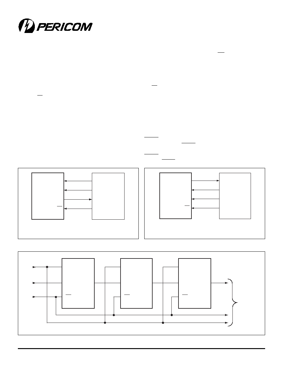
Figure 2. Connections for Microwire
Figure 3. Connections for SPI and QSPI
Figure 4. Daisy-Chained Connection
CS
SCLK
DIN
To
Other
Serial
Devices
CS
SK
SO
SI
I/O
Microwire
Port
PS395A
CS
The DOUT-SI connection is not required for writing to
the PS395A, but may be used for data-echo purposes.
DOUT
DIN
SCLK
MISO
MOSI
SCK
I/O
SPI
Port
PS395A
CS
The DOUT-MISO connection is not required for writing to
the PS395A, but may be used for data-echo purposes.
CPOL = 0, CPHA = 0
SCLK
DIN
DOUT
相關(guān)PDF資料 |
PDF描述 |
|---|---|
| PS395CNB | OCTAL 1-CHANNEL, SGL POLE SGL THROW SWITCH, PDIP24 |
| PS395ENG | OCTAL 1-CHANNEL, SGL POLE SGL THROW SWITCH, PDIP24 |
| PS395CWG | OCTAL 1-CHANNEL, SGL POLE SGL THROW SWITCH, PDSO24 |
| PS395EWG | OCTAL 1-CHANNEL, SGL POLE SGL THROW SWITCH, PDSO24 |
| PS395CPG | OCTAL 1-CHANNEL, SGL POLE SGL THROW SWITCH, PDIP24 |
相關(guān)代理商/技術(shù)參數(shù) |
參數(shù)描述 |
|---|---|
| PS395CNB | 制造商:未知廠家 制造商全稱:未知廠家 功能描述:ANALOG SWITCH|OCTAL|SPST|CMOS|DIP|24PIN|PLASTIC |
| PS395CWG | 制造商:未知廠家 制造商全稱:未知廠家 功能描述:ANALOG SWITCH|OCTAL|SPST|CMOS|SOP|24PIN|PLASTIC |
| PS395ENG | 制造商:未知廠家 制造商全稱:未知廠家 功能描述:ANALOG SWITCH|OCTAL|SPST|CMOS|DIP|24PIN|PLASTIC |
| PS395EWG | 制造商:未知廠家 制造商全稱:未知廠家 功能描述:ANALOG SWITCH|OCTAL|SPST|CMOS|SOP|24PIN|PLASTIC |
| PS396 | 制造商:PERICOM 制造商全稱:Pericom Semiconductor Corporation 功能描述:Precision, 16-Channel 17V Analog Multiplexer |
發(fā)布緊急采購(gòu),3分鐘左右您將得到回復(fù)。