- 您現(xiàn)在的位置:買賣IC網(wǎng) > PDF目錄98060 > PQ60280FTA26PRF-G (SYNQOR INC) 1-OUTPUT DC-DC REG PWR SUPPLY MODULE PDF資料下載
參數(shù)資料
| 型號: | PQ60280FTA26PRF-G |
| 廠商: | SYNQOR INC |
| 元件分類: | 電源模塊 |
| 英文描述: | 1-OUTPUT DC-DC REG PWR SUPPLY MODULE |
| 封裝: | ROHS COMPLIANT, FULL BRICK PACKAGE-18 |
| 文件頁數(shù): | 3/14頁 |
| 文件大?。?/td> | 658K |
| 代理商: | PQ60280FTA26PRF-G |
Product # PQ60280FTA26
Phone 1-888-567-9596
Doc.# 005-2FT628P Rev. C
5/21/08
Page 11
T
Technical S
echnical Specification
pecification
Input:
Output:
Current:
PPackage:
ackage:
36-75 V
28 V
26 A
Full-brick
To increase the output voltage, the user should connect a resistor
between Pin 7 and Pin 8 (SENSE(+) input). For a desired increase
of the nominal output voltage, the value of the resistor should be
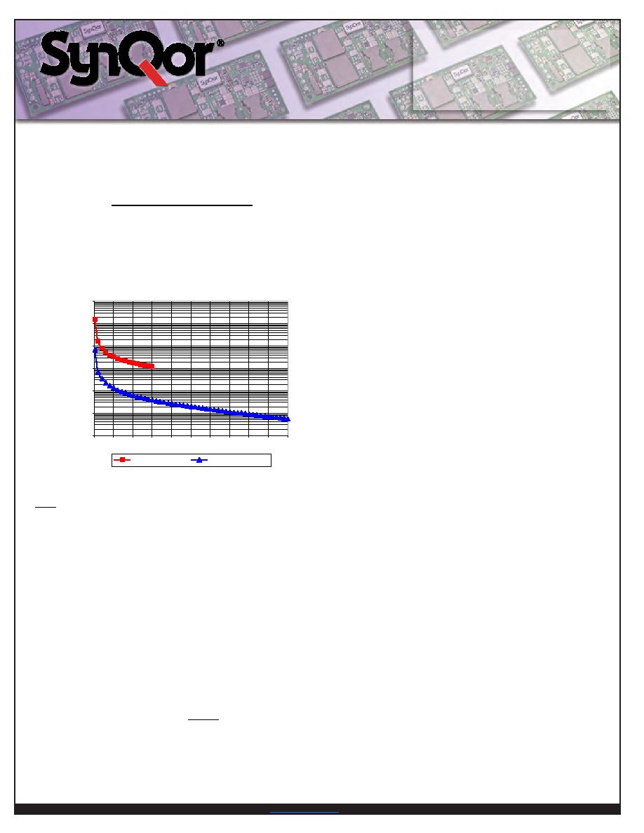
Figure C graphs the relationship between the trim resistor value
and Rtrim-up and Rtrim-down, showing the total range the output
voltage can be trimmed up or down.
Figure C: Trim Graph for 28Vout module
Note: the TRIM feature does not affect the voltage at which the
output over-voltage protection circuit is triggered. Trimming the
output voltage too high may cause the over-voltage protection cir-
cuit to engage, particularly during transients.
It is not necessary for the user to add capacitance at the Trim pin.
The node is internally bypassed to eliminate noise.
Total DC Variation of Vout: For the converter to meet its full
specifications, the maximum variation of the DC value of Vout,
due to both trimming and remote load voltage drops, should not
be greater than that specified for the output voltage trim range.
Current Share (pin 9): The active current share feature allows
for N+1 and parallel applications. To achieve load
sharing,
directly connect the I share pins of multiple units. The load current
will share equally among the multiple units. It is important that
the Vin(-) pins of the sharing units be directly connected and NOT
placed outside of an EMI filter or other impedance path. The volt-
age at the I Share pin will range from 1 to 2.4 volts (at full rated
current), referenced to the primary-side ground, Vin(-)
SYNCHRONIZATION:
The converter’s switching frequency
can be synchronized to an external frequency source that is in the
270 kHz to 330 kHz range. A pulse train at the desired fre-
quency should be applied to the SYNC IN pin (pin 1) with
respect to the INPUT RETURN (pin 6). Its frequency can be any-
where in that range, regardless of the natural frequency of the
power converter. This pulse train should have a duty cycle in the
20% to 80% range. Its low value should be below 0.8V to be
guaranteed to be interpreted as a logic low, and its high value
should be above 2.0V to be guaranteed to be interpreted as a
logic high. The transition time between the two states should be
less than 300ns.
If the converter is not to be synchronized, the SYNC IN pin
should be left open circuit. The converter will then operate in its
free-running mode at a frequency of approximately 300 kHz.
The converter also has a SYNC OUT pin (pin 2). The pulse train
coming out of SYNC OUT has a frequency that matches the
switching frequency of the converter with which it is associated.
This frequency is either the free-running frequency if there is no
synchronization signal at the SYNC IN pin, or the synchroniza-
tion frequency if there is.
1
10
100
1,000
10,000
100,000
1,000,000
0
5
10
15
20
25
30
35
40
45
50
T
ri
m
R
e
s
is
ta
n
c
e
(k
O
h
m
s
)
% Increase in Vout
% Decrease in Vout
(k
W)
Rtrim-up =
16000 + 158.4 x (VDES - VNOM)
VDES - VNOM
相關(guān)PDF資料 |
PDF描述 |
|---|---|
| PQ60280FTA26PNF-G | 1-OUTPUT DC-DC REG PWR SUPPLY MODULE |
| PQ60280FTA26PYF-G | 1-OUTPUT DC-DC REG PWR SUPPLY MODULE |
| PQ60280FTA26NYS-G | 1-OUTPUT DC-DC REG PWR SUPPLY MODULE |
| PQ60480QTA03NRS-G | 1-OUTPUT 144 W DC-DC REG PWR SUPPLY MODULE |
| PQ60480QTA03PYS-G | 1-OUTPUT 144 W DC-DC REG PWR SUPPLY MODULE |
相關(guān)代理商/技術(shù)參數(shù) |
參數(shù)描述 |
|---|---|
| PQ60280FTA26PRS-G | 制造商:SYNQOR 制造商全稱:SYNQOR 功能描述:Full-brick DC/DC Converter |
| PQ60280FTA26PYF-G | 制造商:SYNQOR 制造商全稱:SYNQOR 功能描述:Full-brick DC/DC Converter |
| PQ60280FTA26PYS-G | 制造商:SYNQOR 制造商全稱:SYNQOR 功能描述:Full-brick DC/DC Converter |
| PQ60280FTB26NKF-G | 制造商:SYNQOR 制造商全稱:SYNQOR 功能描述:Full-brick DC/DC Converter |
| PQ60280FTB26NKS-G | 制造商:SYNQOR 制造商全稱:SYNQOR 功能描述:Full-brick DC/DC Converter |
發(fā)布緊急采購,3分鐘左右您將得到回復。