- 您現(xiàn)在的位置:買賣IC網(wǎng) > PDF目錄3894 > PIC17LC43-08I/PQ (Microchip Technology)IC MCU OTP 4KX16 PWM 44-MQFP PDF資料下載
第1頁第2頁第3頁第4頁第5頁第6頁第7頁第8頁第9頁當前第10頁第11頁第12頁第13頁第14頁第15頁第16頁第17頁第18頁第19頁第20頁第21頁第22頁第23頁第24頁第25頁第26頁第27頁第28頁第29頁第30頁第31頁第32頁第33頁第34頁第35頁第36頁第37頁第38頁第39頁第40頁第41頁第42頁第43頁第44頁第45頁第46頁第47頁第48頁第49頁第50頁第51頁第52頁第53頁第54頁第55頁第56頁第57頁第58頁第59頁第60頁第61頁第62頁第63頁第64頁第65頁第66頁第67頁第68頁第69頁第70頁第71頁第72頁第73頁第74頁第75頁第76頁第77頁第78頁第79頁第80頁第81頁第82頁第83頁第84頁第85頁第86頁第87頁第88頁第89頁第90頁第91頁第92頁第93頁第94頁第95頁第96頁第97頁第98頁第99頁第100頁第101頁第102頁第103頁第104頁第105頁第106頁第107頁第108頁第109頁第110頁第111頁第112頁第113頁第114頁第115頁第116頁第117頁第118頁第119頁第120頁第121頁第122頁第123頁第124頁第125頁第126頁第127頁第128頁第129頁第130頁第131頁第132頁第133頁第134頁第135頁第136頁第137頁第138頁第139頁第140頁第141頁第142頁第143頁第144頁第145頁第146頁第147頁第148頁第149頁第150頁第151頁第152頁第153頁第154頁第155頁第156頁第157頁第158頁第159頁第160頁第161頁第162頁第163頁第164頁第165頁第166頁第167頁第168頁第169頁第170頁第171頁第172頁第173頁第174頁第175頁第176頁第177頁第178頁第179頁第180頁第181頁第182頁第183頁第184頁第185頁第186頁第187頁第188頁第189頁第190頁第191頁第192頁第193頁第194頁第195頁第196頁第197頁第198頁第199頁第200頁第201頁第202頁第203頁第204頁第205頁第206頁第207頁第208頁第209頁第210頁第211頁第212頁第213頁第214頁第215頁第216頁第217頁第218頁第219頁第220頁第221頁第222頁第223頁第224頁第225頁第226頁第227頁第228頁第229頁第230頁第231頁第232頁第233頁第234頁第235頁第236頁第237頁第238頁第239頁第240頁第241頁
1996 Microchip Technology Inc.
DS30412C-page 107
PIC17C4X
15.0
INSTRUCTION SET SUMMARY
The PIC17CXX instruction set consists of 58 instruc-
tions. Each instruction is a 16-bit word divided into an
OPCODE and one or more operands. The opcode
species the instruction type, while the operand(s) fur-
ther specify the operation of the instruction. The
PIC17CXX instruction set can be grouped into three
types:
byte-oriented
bit-oriented
literal and control operations.
These formats are shown in Figure 15-1.
Table 15-1 shows the eld descriptions for the
opcodes. These descriptions are useful for under-
standing the opcodes in Table 15-2 and in each spe-
cic instruction descriptions.
byte-oriented instructions, 'f' represents a le regis-
ter designator and 'd' represents a destination designa-
tor. The le register designator species which le
register is to be used by the instruction.
The destination designator species where the result of
the operation is to be placed. If 'd' = '0', the result is
placed in the WREG register. If 'd' = '1', the result is
placed in the le register specied by the instruction.
bit-oriented instructions, 'b' represents a bit eld des-
ignator which selects the number of the bit affected by
the operation, while 'f' represents the number of the le
in which the bit is located.
literal and control operations, 'k' represents an 8- or
11-bit constant or literal value.
The instruction set is highly orthogonal and is grouped
into:
byte-oriented operations
bit-oriented operations
literal and control operations
All instructions are executed within one single instruc-
tion cycle, unless:
a conditional test is true
the program counter is changed as a result of an
instruction
a table read or a table write instruction is exe-
cuted (in this case, the execution takes two
instruction cycles with the second cycle executed
as a NOP)
One instruction cycle consists of four oscillator periods.
Thus, for an oscillator frequency of 25 MHz, the normal
instruction execution time is 160 ns. If a conditional test
is true or the program counter is changed as a result of
an instruction, the instruction execution time is 320 ns.
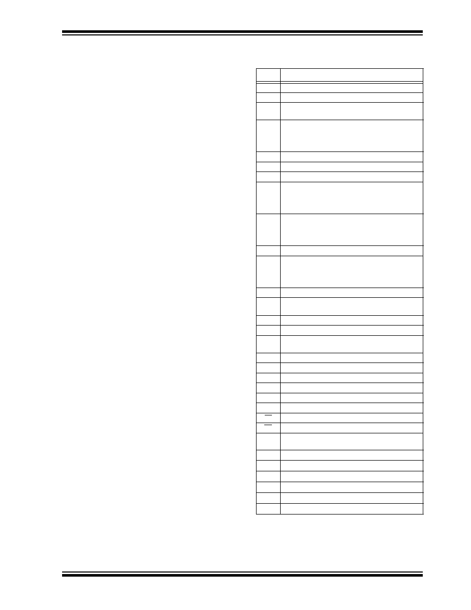
TABLE 15-1:
OPCODE FIELD
DESCRIPTIONS
Field
Description
f
Register le address (00h to FFh)
p
Peripheral register le address (00h to 1Fh)
i
Table pointer control i = '0' (do not change)
i = '1' (increment after instruction execution)
t
Table byte select t = '0' (perform operation on lower
byte)
t = '1' (perform operation on upper byte literal eld,
constant data)
WREG
Working register (accumulator)
b
Bit address within an 8-bit le register
k
Literal eld, constant data or label
x
Don't care location (= '0' or '1')
The assembler will generate code with x = '0'. It is
the recommended form of use for compatibility with
all Microchip software tools.
d
Destination select
0 = store result in WREG
1 = store result in le register f
Default is d = '1'
u
Unused, encoded as '0'
s
Destination select
0 = store result in le register f and in the WREG
1 = store result in le register f
Default is s = '1'
label
Label name
C,DC,
Z,OV
ALU status bits Carry, Digit Carry, Zero, Overow
GLINTD
Global Interrupt Disable bit (CPUSTA<4>)
TBLPTR
Table Pointer (16-bit)
TBLAT
Table Latch (16-bit) consists of high byte (TBLATH)
and low byte (TBLATL)
TBLATL
Table Latch low byte
TBLATH
Table Latch high byte
TOS
Top of Stack
PC
Program Counter
BSR
Bank Select Register
WDT
Watchdog Timer Counter
TO
Time-out bit
PD
Power-down bit
dest
Destination either the WREG register or the speci-
ed register le location
[ ]
Options
( )
Contents
→
Assigned to
< >
Register bit eld
∈
In the set of
italics User dened term (font is courier)
This document was created with FrameMaker404
相關PDF資料 |
PDF描述 |
|---|---|
| PIC17LC43-08I/P | IC MCU OTP 4KX16 PWM 40DIP |
| PIC17LC42AT-08/PQ | IC MCU OTP 2KX16 PWM 44-MQFP |
| PIC17LC42AT-08/L | IC MCU OTP 2KX16 PWM 44PLCC |
| PIC17LC42AT-08I/PQ | IC MCU OTP 2KX16 PWM 44-MQFP |
| PIC17LC42AT-08I/L | IC MCU OTP 2KX16 PWM 44PLCC |
相關代理商/技術參數(shù) |
參數(shù)描述 |
|---|---|
| PIC17LC43T-08/L | 功能描述:8位微控制器 -MCU 8KB 454 RAM 33 I/O RoHS:否 制造商:Silicon Labs 核心:8051 處理器系列:C8051F39x 數(shù)據(jù)總線寬度:8 bit 最大時鐘頻率:50 MHz 程序存儲器大小:16 KB 數(shù)據(jù) RAM 大小:1 KB 片上 ADC:Yes 工作電源電壓:1.8 V to 3.6 V 工作溫度范圍:- 40 C to + 105 C 封裝 / 箱體:QFN-20 安裝風格:SMD/SMT |
| PIC17LC43T-08/PQ | 功能描述:8位微控制器 -MCU 8KB 454 RAM 33 I/O RoHS:否 制造商:Silicon Labs 核心:8051 處理器系列:C8051F39x 數(shù)據(jù)總線寬度:8 bit 最大時鐘頻率:50 MHz 程序存儲器大小:16 KB 數(shù)據(jù) RAM 大小:1 KB 片上 ADC:Yes 工作電源電壓:1.8 V to 3.6 V 工作溫度范圍:- 40 C to + 105 C 封裝 / 箱體:QFN-20 安裝風格:SMD/SMT |
| PIC17LC43T-08/PT | 功能描述:8位微控制器 -MCU 8KB 454 RAM 33 I/O RoHS:否 制造商:Silicon Labs 核心:8051 處理器系列:C8051F39x 數(shù)據(jù)總線寬度:8 bit 最大時鐘頻率:50 MHz 程序存儲器大小:16 KB 數(shù)據(jù) RAM 大小:1 KB 片上 ADC:Yes 工作電源電壓:1.8 V to 3.6 V 工作溫度范圍:- 40 C to + 105 C 封裝 / 箱體:QFN-20 安裝風格:SMD/SMT |
| PIC17LC43T-08I/L | 功能描述:8位微控制器 -MCU LOW PWR RoHS:否 制造商:Silicon Labs 核心:8051 處理器系列:C8051F39x 數(shù)據(jù)總線寬度:8 bit 最大時鐘頻率:50 MHz 程序存儲器大小:16 KB 數(shù)據(jù) RAM 大小:1 KB 片上 ADC:Yes 工作電源電壓:1.8 V to 3.6 V 工作溫度范圍:- 40 C to + 105 C 封裝 / 箱體:QFN-20 安裝風格:SMD/SMT |
| PIC17LC43T-08I/PQ | 功能描述:8位微控制器 -MCU 8KB 454 RAM 33 I/O RoHS:否 制造商:Silicon Labs 核心:8051 處理器系列:C8051F39x 數(shù)據(jù)總線寬度:8 bit 最大時鐘頻率:50 MHz 程序存儲器大小:16 KB 數(shù)據(jù) RAM 大小:1 KB 片上 ADC:Yes 工作電源電壓:1.8 V to 3.6 V 工作溫度范圍:- 40 C to + 105 C 封裝 / 箱體:QFN-20 安裝風格:SMD/SMT |
發(fā)布緊急采購,3分鐘左右您將得到回復。