- 您現(xiàn)在的位置:買賣IC網(wǎng) > PDF目錄299771 > PIC16C74T-20I/TQ 8-BIT, OTPROM, 20 MHz, RISC MICROCONTROLLER, PQFP44 PDF資料下載
參數(shù)資料
| 型號(hào): | PIC16C74T-20I/TQ |
| 元件分類: | 微控制器/微處理器 |
| 英文描述: | 8-BIT, OTPROM, 20 MHz, RISC MICROCONTROLLER, PQFP44 |
| 封裝: | 10 X 10 MM, PLASTIC, TQFP-44 |
| 文件頁數(shù): | 115/289頁 |
| 文件大小: | 2211K |
| 代理商: | PIC16C74T-20I/TQ |
第1頁第2頁第3頁第4頁第5頁第6頁第7頁第8頁第9頁第10頁第11頁第12頁第13頁第14頁第15頁第16頁第17頁第18頁第19頁第20頁第21頁第22頁第23頁第24頁第25頁第26頁第27頁第28頁第29頁第30頁第31頁第32頁第33頁第34頁第35頁第36頁第37頁第38頁第39頁第40頁第41頁第42頁第43頁第44頁第45頁第46頁第47頁第48頁第49頁第50頁第51頁第52頁第53頁第54頁第55頁第56頁第57頁第58頁第59頁第60頁第61頁第62頁第63頁第64頁第65頁第66頁第67頁第68頁第69頁第70頁第71頁第72頁第73頁第74頁第75頁第76頁第77頁第78頁第79頁第80頁第81頁第82頁第83頁第84頁第85頁第86頁第87頁第88頁第89頁第90頁第91頁第92頁第93頁第94頁第95頁第96頁第97頁第98頁第99頁第100頁第101頁第102頁第103頁第104頁第105頁第106頁第107頁第108頁第109頁第110頁第111頁第112頁第113頁第114頁當(dāng)前第115頁第116頁第117頁第118頁第119頁第120頁第121頁第122頁第123頁第124頁第125頁第126頁第127頁第128頁第129頁第130頁第131頁第132頁第133頁第134頁第135頁第136頁第137頁第138頁第139頁第140頁第141頁第142頁第143頁第144頁第145頁第146頁第147頁第148頁第149頁第150頁第151頁第152頁第153頁第154頁第155頁第156頁第157頁第158頁第159頁第160頁第161頁第162頁第163頁第164頁第165頁第166頁第167頁第168頁第169頁第170頁第171頁第172頁第173頁第174頁第175頁第176頁第177頁第178頁第179頁第180頁第181頁第182頁第183頁第184頁第185頁第186頁第187頁第188頁第189頁第190頁第191頁第192頁第193頁第194頁第195頁第196頁第197頁第198頁第199頁第200頁第201頁第202頁第203頁第204頁第205頁第206頁第207頁第208頁第209頁第210頁第211頁第212頁第213頁第214頁第215頁第216頁第217頁第218頁第219頁第220頁第221頁第222頁第223頁第224頁第225頁第226頁第227頁第228頁第229頁第230頁第231頁第232頁第233頁第234頁第235頁第236頁第237頁第238頁第239頁第240頁第241頁第242頁第243頁第244頁第245頁第246頁第247頁第248頁第249頁第250頁第251頁第252頁第253頁第254頁第255頁第256頁第257頁第258頁第259頁第260頁第261頁第262頁第263頁第264頁第265頁第266頁第267頁第268頁第269頁第270頁第271頁第272頁第273頁第274頁第275頁第276頁第277頁第278頁第279頁第280頁第281頁第282頁第283頁第284頁第285頁第286頁第287頁第288頁第289頁
1997 Microchip Technology Inc.
DS30390E-page 201
PIC16C7X
Applicable Devices 72 73 73A 74 74A 76 77
19.0
ELECTRICAL CHARACTERISTICS FOR PIC16C73A/74A
Absolute Maximum Ratings
Ambient temperature under bias..................................................................................................................-55 to +125C
Storage temperature ............................................................................................................................... -65C to +150C
Voltage on any pin with respect to VSS (except VDD, MCLR. and RA4)........................................... -0.3V to (VDD + 0.3V)
Voltage on VDD with respect to VSS ............................................................................................................ -0.3 to +7.5V
Voltage on MCLR with respect to VSS (Note 2) ................................................................................................. 0 to +14V
Voltage on RA4 with respect to Vss ................................................................................................................... 0 to +14V
Total power dissipation (Note 1).................................................................................................................................1.0W
Maximum current out of VSS pin ............................................................................................................................300 mA
Maximum current into VDD pin ...............................................................................................................................250 mA
Input clamp current, IIK (VI < 0 or VI > VDD)
.....................................................................................................................± 20 mA
Output clamp current, IOK (VO < 0 or VO > VDD)
..............................................................................................................± 20 mA
Maximum output current sunk by any I/O pin...........................................................................................................25 mA
Maximum output current sourced by any I/O pin .....................................................................................................25 mA
Maximum current sunk by PORTA, PORTB, and PORTE (combined) (Note 3).....................................................200 mA
Maximum current sourced by PORTA, PORTB, and PORTE (combined) (Note 3) ...............................................200 mA
Maximum current sunk by PORTC and PORTD (combined) (Note 3) ...................................................................200 mA
Maximum current sourced by PORTC and PORTD (combined) (Note 3)..............................................................200 mA
Note 1: Power dissipation is calculated as follows: Pdis = VDD x {IDD -
∑ IOH} + ∑ {(VDD - VOH) x IOH} + ∑(VOl x IOL)
Note 2: Voltage spikes below VSS at the MCLR pin, inducing currents greater than 80 mA, may cause latch-up. Thus,
a series resistor of 50-100
should be used when applying a “l(fā)ow” level to the MCLR pin rather than pulling
this pin directly to VSS.
Note 3: PORTD and PORTE are not implemented on the PIC16C73A.
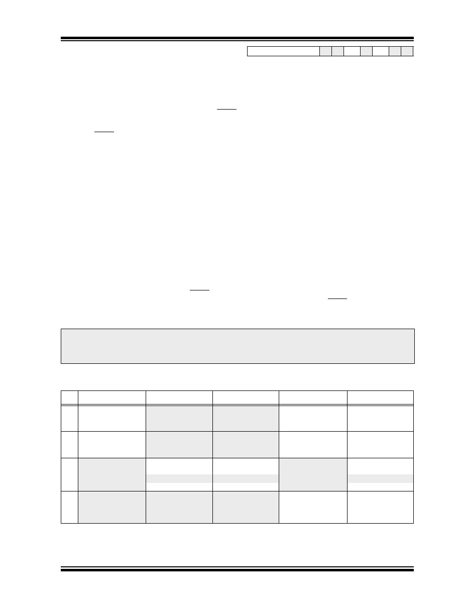
TABLE 19-1:
CROSS REFERENCE OF DEVICE SPECS FOR OSCILLATOR CONFIGURATIONS
AND FREQUENCIES OF OPERATION (COMMERCIAL DEVICES)
NOTICE: Stresses above those listed under “Absolute Maximum Ratings” may cause permanent damage to the
device. This is a stress rating only and functional operation of the device at those or any other conditions above those
indicated in the operation listings of this specication is not implied. Exposure to maximum rating conditions for
extended periods may affect device reliability.
OSC
PIC16C73A-04
PIC16C74A-04
PIC16C73A-10
PIC16C74A-10
PIC16C73A-20
PIC16C74A-20
PIC16LC73A-04
PIC16LC74A-04
JW Devices
RC
VDD: 4.0V to 6.0V
IDD: 5 mA max. at 5.5V
IPD: 16
A max. at 4V
Freq: 4 MHz max.
VDD: 4.5V to 5.5V
IDD: 2.7 mA typ. at 5.5V
IPD: 1.5
A typ. at 4V
Freq: 4 MHz max.
VDD: 4.5V to 5.5V
IDD: 2.7 mA typ. at 5.5V
IPD: 1.5
A typ. at 4V
Freq: 4 MHz max.
VDD: 2.5V to 6.0V
IDD: 3.8 mA max. at 3.0V
IPD: 5
A max. at 3V
Freq: 4 MHz max.
VDD: 4.0V to 6.0V
IDD: 5 mA max. at 5.5V
IPD: 16
A max. at 4V
Freq: 4 MHz max.
XT
VDD: 4.0V to 6.0V
IDD: 5 mA max. at 5.5V
IPD: 16
A max. at 4V
Freq: 4 MHz max.
VDD: 4.5V to 5.5V
IDD: 2.7 mA typ. at 5.5V
IPD: 1.5
A typ. at 4V
Freq: 4 MHz max.
VDD: 4.5V to 5.5V
IDD: 2.7 mA typ. at 5.5V
IPD: 1.5
A typ. at 4V
Freq: 4 MHz max.
VDD: 2.5V to 6.0V
IDD: 3.8 mA max. at 3.0V
IPD: 5
A max. at 3V
Freq: 4 MHz max.
VDD: 4.0V to 6.0V
IDD: 5 mA max. at 5.5V
IPD: 16
A max. at 4V
Freq: 4 MHz max.
HS
VDD: 4.5V to 5.5V
Not recommended for
use in HS mode
VDD: 4.5V to 5.5V
IDD: 13.5 mA typ. at 5.5V
IDD: 10 mA max. at 5.5V
IDD: 20 mA max. at 5.5V
IPD: 1.5
A typ. at 4.5V
IPD: 1.5
A typ. at 4.5V
IPD: 1.5
A typ. at 4.5V
IPD: 1.5
A typ. at 4.5V
Freq: 4 MHz max.
Freq: 10 MHz max.
Freq: 20 MHz max.
LP
VDD: 4.0V to 6.0V
IDD: 52.5
A typ. at
32 kHz, 4.0V
IPD: 0.9
A typ. at 4.0V
Freq: 200 kHz max.
Not recommended for
use in LP mode
Not recommended for
use in LP mode
VDD: 2.5V to 6.0V
IDD: 48
A max. at
32 kHz, 3.0V
IPD: 5.0
A max. at 3.0V
Freq: 200 kHz max.
VDD: 2.5V to 6.0V
IDD: 48
A max. at
32 kHz, 3.0V
IPD: 5.0
A max. at 3.0V
Freq: 200 kHz max.
The shaded sections indicate oscillator selections which are tested for functionality, but not for MIN/MAX specications.
It is recommended that the user select the device type that ensures the specications required.
相關(guān)PDF資料 |
PDF描述 |
|---|---|
| PIC16C923T-04I/PT | 8-BIT, OTPROM, 4 MHz, RISC MICROCONTROLLER, PQFP64 |
| PIC16C925/L | 8-BIT, OTPROM, 20 MHz, RISC MICROCONTROLLER, PQCC68 |
| PIC16C925/PT | 8-BIT, OTPROM, 20 MHz, RISC MICROCONTROLLER, PQFP64 |
| PIC16LC926-I/PT | 8-BIT, OTPROM, 10 MHz, RISC MICROCONTROLLER, PQFP64 |
| PIC16F1518-I/SO | 8-BIT, FLASH, RISC MICROCONTROLLER, PDSO28 |
相關(guān)代理商/技術(shù)參數(shù) |
參數(shù)描述 |
|---|---|
| PIC16C76/JW | 功能描述:8位微控制器 -MCU 14KB 368 RAM 22 I/O RoHS:否 制造商:Silicon Labs 核心:8051 處理器系列:C8051F39x 數(shù)據(jù)總線寬度:8 bit 最大時(shí)鐘頻率:50 MHz 程序存儲(chǔ)器大小:16 KB 數(shù)據(jù) RAM 大小:1 KB 片上 ADC:Yes 工作電源電壓:1.8 V to 3.6 V 工作溫度范圍:- 40 C to + 105 C 封裝 / 箱體:QFN-20 安裝風(fēng)格:SMD/SMT |
| PIC16C76-04/SO | 功能描述:8位微控制器 -MCU 14KB 368 RAM 22 I/O RoHS:否 制造商:Silicon Labs 核心:8051 處理器系列:C8051F39x 數(shù)據(jù)總線寬度:8 bit 最大時(shí)鐘頻率:50 MHz 程序存儲(chǔ)器大小:16 KB 數(shù)據(jù) RAM 大小:1 KB 片上 ADC:Yes 工作電源電壓:1.8 V to 3.6 V 工作溫度范圍:- 40 C to + 105 C 封裝 / 箱體:QFN-20 安裝風(fēng)格:SMD/SMT |
| PIC16C76-04/SO | 制造商:Microchip Technology Inc 功能描述:8BIT CMOS MCU SMD 16C76 SOIC28 |
| PIC16C76-04/SP | 功能描述:8位微控制器 -MCU 14KB 368 RAM 22 I/O RoHS:否 制造商:Silicon Labs 核心:8051 處理器系列:C8051F39x 數(shù)據(jù)總線寬度:8 bit 最大時(shí)鐘頻率:50 MHz 程序存儲(chǔ)器大小:16 KB 數(shù)據(jù) RAM 大小:1 KB 片上 ADC:Yes 工作電源電壓:1.8 V to 3.6 V 工作溫度范圍:- 40 C to + 105 C 封裝 / 箱體:QFN-20 安裝風(fēng)格:SMD/SMT |
| PIC16C76-04/SP | 制造商:Microchip Technology Inc 功能描述:IC 8BIT CMOS MCU 16C76 SDIL28 |
發(fā)布緊急采購,3分鐘左右您將得到回復(fù)。