- 您現(xiàn)在的位置:買賣IC網(wǎng) > PDF目錄299640 > PDSP16350/B0/AC (ZARLINK SEMICONDUCTOR INC) 34-BIT, DSP-NUM CONTROLLED OSCILLATOR, CPGA84 PDF資料下載
參數(shù)資料
| 型號: | PDSP16350/B0/AC |
| 廠商: | ZARLINK SEMICONDUCTOR INC |
| 元件分類: | 數(shù)字信號處理外設(shè) |
| 英文描述: | 34-BIT, DSP-NUM CONTROLLED OSCILLATOR, CPGA84 |
| 封裝: | PGA-84 |
| 文件頁數(shù): | 3/13頁 |
| 文件大小: | 256K |
| 代理商: | PDSP16350/B0/AC |
PDSP16350
10
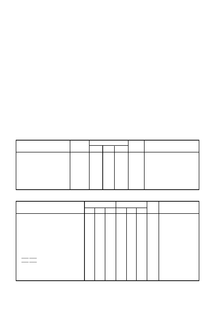
Characteristic
Output high voltage
Output low voltage
Input high voltage
Input low voltage
Input leakage current
Input capacitance
Output leakage current
Output S/C current
NOTES
1. Exceeding these ratings may cause permanent damage.
Functional operation under these conditions is not implied.
2. Maximum dissipation or 1 second should not be ex-
ceeded, only one output to be tested at any one time.
3. Exposure to absolute maximum ratings for extended peri-
ods may affect device reliablity.
4. Vcc = Max, Outputs Unloaded, Clock Freq = Max.
5. CMOS levels are defined as
VIH = VDD - 0.5v
VIL = +0.5v
6. Current is defined as positive into the device.
7. The
JC data assumes that heat is extracted from the top
face of the package.
ABSOLUTE MAXIMUM RATINGS (Note 1)
Supply voltage Vcc
-0.5V to 7.0V
Input voltage V
IN
-0.5V to Vcc + 0.5V
Output voltage V
OUT
-0.5V to Vcc + 0.5V
Clamp diode current per pin I
K (see note 2)
18mA
Static discharge voltage (HMB)
500V
Storage temperature T
S
-65
°C to 150°C
Ambient temperature with power applied T
AMB
Military
-55
°C to +125°C
Industrial
-40
°C to 85°C
Junction temperature
150
°C
Package power dissipation
3500mW
Thermal resistances
Junction to Case
JC
5
°C/W
Min.
2.4
-
3.0
-
-10
-50
40
Max.
-
0.4
-
0.8
+10
+50
250
Conditions
I
OH = 4mA
I
OL = -4mA
GND < V
IN < VCC
GND < V
OUT < VCC
V
CC = Max
Units
V
A
pF
A
mA
Symbol
V
OH
V
OL
V
IH
V
IL
I
IN
C
IN
I
OZ
I
SC
Value
Typ.
10
Characteristic
Industrial
Military
Units
Conditions
Min.
Typ.
Max.
Min.
Typ.
Max.
D33:0 signal setup to clock rising edge
15
-
15
-
ns
D33:0 signal hold after clock rising edge
4
-
4
-
ns
CEN setup to clock rising edge
20
-
20
-
ns
CEN hold after clock rising edge
0
-
0
-
ns
JUMP, RES setup to clock rising edge
10
-
10
-
ns
JUMP hold after clock rising edge
6
-
6
-
ns
RES hold after clock rising edge
8
-
8
-
ns
Clock rising edge to output valid
5
30
5
30
ns
30pF
Clock freq
DC
20
DC
20
MHz
Clock High Time
15
-
15
-
ns
Clock Low Time
20
-
20
-
ns
OES,OEC low to data valid
-
20
-
20
ns
30pF
OES,OEC high to data high impedance
-
20
-
20
ns
30pF
Pipeline delay VIN to VOUT
31
CLKs
Vcc Current (CMOS inputs)
-
430
-
450
mA
See Note 4
Vcc Current (TTL inputs)
-
460
-
500
mA
See Note 4
Switching Characteristics
ELECTRICAL CHARACTERISTICS
Operating Conditions (unless otherwise stated)
Commercial: T
AMB = 0°C to +70°C TJ(MAX) = 95°C
V
CC = 5.0V±5% Ground = 0V
Industrial: T
AMB = -40°C to +85°C TJ(MAX) = 110°C
V
CC = 5.0V±10% Ground = 0V
Military: T
AMB = -55°C to +125°C TJ(MAX) = 150°C
V
CC = 5.0V±10% Ground = 0V
Static Characteristics
相關(guān)PDF資料 |
PDF描述 |
|---|---|
| PDSP16488AMAACBR | 16-BIT, DSP-CONVOLVER, CPGA84 |
| PE-0402CD2N2KTT | 1 ELEMENT, 0.0022 uH, CERAMIC-CORE, GENERAL PURPOSE INDUCTOR, SMD |
| PE-0402CD6N2JTT | 1 ELEMENT, 0.0062 uH, CERAMIC-CORE, GENERAL PURPOSE INDUCTOR, SMD |
| PE-0805CX470KBT | 1 ELEMENT, 0.047 uH, CERAMIC-CORE, GENERAL PURPOSE INDUCTOR, SMD |
| PE-0805CX681KBT | 1 ELEMENT, 0.68 uH, CERAMIC-CORE, GENERAL PURPOSE INDUCTOR, SMD |
相關(guān)代理商/技術(shù)參數(shù) |
參數(shù)描述 |
|---|---|
| PDSP16350B0GC | 制造商:未知廠家 制造商全稱:未知廠家 功能描述:Trigonometric Function Generator |
| PDSP16350C0AC | 制造商:未知廠家 制造商全稱:未知廠家 功能描述:Trigonometric Function Generator |
| PDSP16350C0GC | 制造商:未知廠家 制造商全稱:未知廠家 功能描述:Trigonometric Function Generator |
| PDSP16401 | 制造商:未知廠家 制造商全稱:未知廠家 功能描述:Analog IC |
| PDSP16401A | 制造商:未知廠家 制造商全稱:未知廠家 功能描述:Analog IC |
發(fā)布緊急采購,3分鐘左右您將得到回復(fù)。