- 您現在的位置:買賣IC網 > PDF目錄367815 > PCF2113WU2 (NXP Semiconductors N.V.) LCD controllers/drivers PDF資料下載
參數資料
| 型號: | PCF2113WU2 |
| 廠商: | NXP Semiconductors N.V. |
| 英文描述: | LCD controllers/drivers |
| 中文描述: | LCD控制器/驅動器 |
| 文件頁數: | 9/72頁 |
| 文件大?。?/td> | 332K |
| 代理商: | PCF2113WU2 |
第1頁第2頁第3頁第4頁第5頁第6頁第7頁第8頁當前第9頁第10頁第11頁第12頁第13頁第14頁第15頁第16頁第17頁第18頁第19頁第20頁第21頁第22頁第23頁第24頁第25頁第26頁第27頁第28頁第29頁第30頁第31頁第32頁第33頁第34頁第35頁第36頁第37頁第38頁第39頁第40頁第41頁第42頁第43頁第44頁第45頁第46頁第47頁第48頁第49頁第50頁第51頁第52頁第53頁第54頁第55頁第56頁第57頁第58頁第59頁第60頁第61頁第62頁第63頁第64頁第65頁第66頁第67頁第68頁第69頁第70頁第71頁第72頁
2001 Dec 19
9
Philips Semiconductors
Product specification
LCD controllers/drivers
PCF2113x
7
FUNCTIONAL DESCRIPTION
7.1
LCD supply voltage generator
The LCD supply voltage may be generated on-chip. The
V
LCD
generator is controlled by two internal 6-bit registers:
V
A
and V
B
. The nominal LCD operating voltage at room
temperature is given by the relationship:
V
OP(nom)
= (integer value of register
×
0.08) + 1.82
7.1.1
P
ROGRAMMING RANGES
Programmed value: 1 to 63. Voltage: 1.90 to 6.86 V.
T
ref
= 27
°
C.
Values producing more than 6.5 V at operating
temperature are not allowed.
Operation above this
voltage may damage the device. When programming the
operating voltage the V
LCD
tolerance and temperature
coefficient must be taken into account.
Values below 2.2 V are below the specified operating
range of the chip and are therefore not allowed.
Value 0 for V
A
and V
B
switches the generator off
(i.e. V
A
= 0 in character mode, V
B
= 0 in icon mode).
Usually register V
A
is programmed with the voltage for
character mode and register V
B
with the voltage for icon
mode.
When V
LCD
is generated on-chip the V
LCD
pins should be
decoupled to V
SS
with a suitable capacitor.
The generated V
LCD
is independent of V
DD
and is
temperature compensated. When the V
LCD
generator and
the direct mode are switched off, an external voltage may
be supplied at connected pins V
LCD1
and V
LCD2
. V
LCD1
and
V
LCD2
may be higher or lower than V
DD2
.
During direct mode (program DM register bit) the internal
V
LCD
generator is turned off and the V
LCD2
output voltage
is directly connected to V
DD2
. This reduces the current
consumption during icon mode and Mux 1 : 9 (depending
on V
DD2
value and LCD liquid properties).
The V
LCD
generator ensures that, as long as V
DD
is in the
valid range (2.2 to 4 V), the required peak voltage
V
OP
= 6.5 V can be generated at any time.
7.2
LCD bias voltage generator
The intermediate bias voltages for the LCD display are
also generated on-chip. This removes the need for an
external resistive bias chain and significantly reduces the
system current consumption. The optimum value of V
LCD
depends on the multiplex rate, the LCD threshold voltage
(V
th
) and the number of bias levels. Using a 5-level bias
scheme for 1 : 18 maximum rate allows V
LCD
< 5 V for
most LCD liquids. The intermediate bias levels for the
different multiplex rates are shown in Table 1. These bias
levels are automatically set to the given values when
switching to the corresponding multiplex rate.
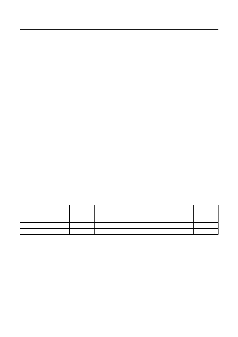
Table 1
Bias levels as a function of multiplex rate; note 1
Note
1.
The values in the table are given relative to V
LCD
V
SS
, e.g.
3
/
4
means
3
/
4
×
(V
LCD
V
SS
).
MULTIPLEX
RATE
NUMBER
OF LEVELS
V
1
V
2
V
3
V
4
V
5
V
6
1 : 18
1 : 9
1 : 2
5
5
4
V
LCD
V
LCD
V
LCD
3
/
4
3
/
4
2
/
3
1
/
2
1
/
2
2
/
3
1
/
2
1
/
2
1
/
3
1
/
4
1
/
4
1
/
3
V
SS
V
SS
V
SS
相關PDF資料 |
PDF描述 |
|---|---|
| PCF2113F2 | LCD controller/driver(LCD控制器/驅動器) |
| PCF211310 | LCD controller/driver(LCD控制器/驅動器) |
| PCF21132 | LCD controller/driver(LCD控制器/驅動器) |
| PCF211410 | LCD controller/drivers(LCD控制器/驅動器) |
| PCF2116AHZ | JT 66C 66#22D PIN RECP |
相關代理商/技術參數 |
參數描述 |
|---|---|
| PCF2113WUF4 | 制造商:PHILIPS 制造商全稱:NXP Semiconductors 功能描述:LCD controllers/drivers |
| PCF2113X | 制造商:PHILIPS 制造商全稱:NXP Semiconductors 功能描述:LCD controllers/drivers |
| PCF2114AH | 制造商:未知廠家 制造商全稱:未知廠家 功能描述:LCD Display Driver |
| PCF2114AU | 制造商:未知廠家 制造商全稱:未知廠家 功能描述:LCD Display Driver |
| PCF2114AU/10 | 制造商:PHILIPS 制造商全稱:NXP Semiconductors 功能描述:LCD controller/drivers |
發(fā)布緊急采購,3分鐘左右您將得到回復。