- 您現(xiàn)在的位置:買賣IC網(wǎng) > PDF目錄224662 > PAC80 (Lattice Semiconductor Corporation) In-System Programmable Analog Circuit PDF資料下載
參數(shù)資料
| 型號: | PAC80 |
| 廠商: | Lattice Semiconductor Corporation |
| 英文描述: | In-System Programmable Analog Circuit |
| 中文描述: | 在系統(tǒng)可編程模擬電路 |
| 文件頁數(shù): | 17/19頁 |
| 文件大小: | 342K |
| 代理商: | PAC80 |
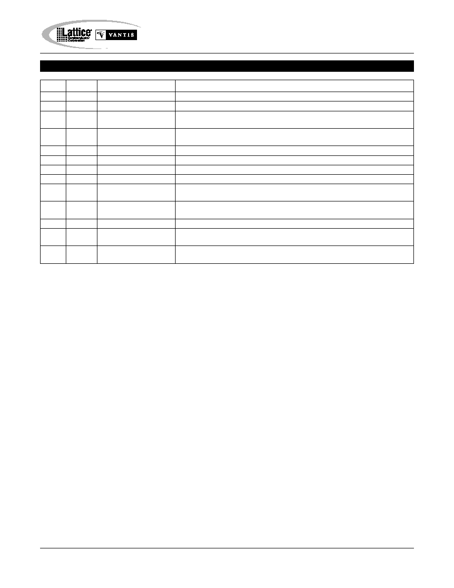
Specifications ispPAC80
7
Pin(s)
Symbol
Name
Description
1
TMS
Test Mode Select
Serial interface logic mode select pin (input). JTAG interface mode only.
2
TCK
Test Clock
Serial interface logic clock pin (input). JTAG interface mode only.
3
TDI
Test Data In
Serial interface logic pin (input) for both JTAG and SPI operation modes.
Input data valid on rising edge of TCK (JTAG), or on rising edge of CS (SPI).
4
TDO
Test Data Out
Serial interface logic pin (output) for both JTAG and SPI operation modes.
Input data valid on falling edge of TCK (JTAG), or on rising edge of CS (SPI).
5
CS
Chip Select
Chip select logic input pin. SPI data latch.
6
CAL
Auto-Calibrate
Digital pin (input). Commands an auto-calibration sequence on a rising edge.
7
ENSPI
Enable SPI Mode
Enable SPI logic input pin. When high, causes serial port to run in SPI mode.
8
GND
Ground
Ground pin. Should normally be connected to the analog ground plane.
9
VREFout
Common-Mode
Common-mode voltage reference output pin (+2.5V nominal). Must be
Reference
bypassed to GND with a 1
F capacitor.
10, 11
IN
Inputs (+ or -)
Differential input pins, using two pins (e.g., IN+ and IN-). Plus or minus
components of VIN, where differential VIN = VIN+ - VIN-.
12, 15
TEST
Test Pin
Test pin. Connect to GND for proper circuit operation.
13, 14
OUT
Outputs (+ or -)
Differential output pins, using two pins (e.g., OUT+ and OUT-).
Complementary with respect to VREFOUT. Differential VOUT = VOUT+ - VOUT-.
16
VS
Supply Voltage
Analog supply voltage pin (5V nominal). Should be bypassed to GND with 1
F
and .01
F capacitors.
Pin Descriptions
Connection Notes
1. All inputs and outputs are labeled with plus (+) and minus (-) signs. Polarity is labeled for reference and can be
selected externally by reversing pin connections.
2. All analog output pins are “hard-wired” to internal output devices and should be left open if not used. VOUT+ and
VOUT- should not be tied together as unnecessary power will be dissipated.
3. When the signal input is single-ended, the other half of the unused differential input must be connected to a DC
common-mode reference (usually VREFOUT, 2.5V).
相關(guān)PDF資料 |
PDF描述 |
|---|---|
| PACE1754-20PGMB | SPECIALTY MICROPROCESSOR CIRCUIT, CPGA68 |
| PAL16R8ANC | Progammable Array Logic Series 24 (PAL Series 24) |
| PAL16R8AVC | Progammable Array Logic Series 24 (PAL Series 24) |
| PAL18C1AN | Progammable Array Logic Series 24 (PAL Series 24) |
| PAL18C1ANC | Progammable Array Logic Series 24 (PAL Series 24) |
相關(guān)代理商/技術(shù)參數(shù) |
參數(shù)描述 |
|---|---|
| PAC80/81-EV | 功能描述:可編程邏輯 IC 開發(fā)工具 ispPAC80 & ispPAC81 Eval Brd RoHS:否 制造商:Altera Corporation 產(chǎn)品:Development Kits 類型:FPGA 工具用于評估:5CEFA7F3 接口類型: 工作電源電壓: |
| P-AC-832-2 | 制造商:PSM International 功能描述: |
| P-AC84RZSZ0U | 制造商:Panasonic Industrial Devices 功能描述:AGITATOR SUB:AC84RBZDZ000 |
| P-AC88RYUZV06 | 制造商:Panasonic Industrial Devices 功能描述:BRUSH |
| PAC91 | 功能描述:測試引線 PRINT ADAPTER CABL RoHS:否 制造商:Pomona Electronics 設(shè)備類型:Patch Cords 連接器類型:Banana plug (stackable) on both ends 長度:60 in 顏色:Black |
發(fā)布緊急采購,3分鐘左右您將得到回復(fù)。