- 您現(xiàn)在的位置:買賣IC網(wǎng) > PDF目錄383735 > PAC7136 (飛思卡爾半導體(中國)有限公司) Microcontroller Family Hardware Specifications PDF資料下載
參數(shù)資料
| 型號: | PAC7136 |
| 廠商: | 飛思卡爾半導體(中國)有限公司 |
| 英文描述: | Microcontroller Family Hardware Specifications |
| 中文描述: | 微控制器系列硬件規(guī)格 |
| 文件頁數(shù): | 5/56頁 |
| 文件大小: | 471K |
| 代理商: | PAC7136 |
第1頁第2頁第3頁第4頁當前第5頁第6頁第7頁第8頁第9頁第10頁第11頁第12頁第13頁第14頁第15頁第16頁第17頁第18頁第19頁第20頁第21頁第22頁第23頁第24頁第25頁第26頁第27頁第28頁第29頁第30頁第31頁第32頁第33頁第34頁第35頁第36頁第37頁第38頁第39頁第40頁第41頁第42頁第43頁第44頁第45頁第46頁第47頁第48頁第49頁第50頁第51頁第52頁第53頁第54頁第55頁第56頁
Electrical Characteristics
MAC7100 Microcontroller Family Hardware Specifications, Rev. 1.2
Preliminary
Freescale Semiconductor
5
3.3
ESD Protection and Latch-up Immunity
All ESD testing is in conformity with CDF-AEC-Q100 Stress test qualification for Automotive Grade
Integrated Circuits. During the device qualification ESD stresses were performed for the Human Body
Model (HBM), the Machine Model (MM) and the Charge Device Model.
A device is defined as a failure if after exposure to ESD pulses the device no longer meets the device
specification. Complete DC parametric and functional testing is performed per the applicable device
specification at room temperature followed by hot temperature, unless specified otherwise.
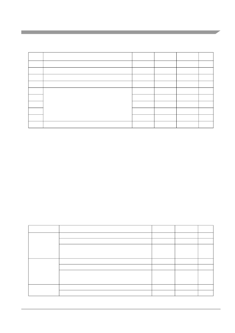
A9
Voltage difference V
DD
A – V
RH
V
DD
A – V
RH
–0.3
+6.0
V
A10
Digital I/O Input Voltage
V
IN
–0.3
+6.0
V
A11
XFC, EXTAL, XTAL inputs
V
ILV
–0.3
+3.0
V
A12
TEST input
V
TEST
–0.3
—
2
V
Instantaneous Maximum Current
3
A13
Single pin limit for XFC, EXTAL, XTAL
4
I
DL
I
D
I
DA
I
DT
T
stg
–25
+25
mA
A14
Single pin limit for all digital I/O pins
5
–25
+25
mA
A15
Single pin limit for all analog input pins
5
–25
+25
mA
A16
Single pin limit for TEST
2
–0.25
0
mA
A17
Storage Temperature Range
–65
+155
°
C
NOTES:
1. The device contains an internal voltage regulator to generate the logic and PLL supply from the I/O supply. The
absolute maximum ratings apply when the device is powered from an external source.
2. This pin is clamped low to V
SS
X, but not clamped high, and must be tied low in applications.
3. Input must be current limited to the value specified. To determine the value of the required current-limiting resistor,
use the larger of the calculated values using V
POSCLAMP
= V
DD
A + 0.3V and V
NEGCLAMP
= –0.3 V.
4. These pins are internally clamped to V
SS
PLL and V
DD
PLL.
5. All I/O pins are internally clamped to V
SS
X and V
DD
X, V
SS
R and V
DD
R or V
SS
A and V
DD
A.
Table 5. ESD and Latch-up Test Conditions
Model
Description
Symbol
Value
Unit
Human Body
Series Resistance
Storage Capacitance
Number of Pulses per pin
positive
negative
Series Resistance
Storage Capacitance
Number of Pulse per pin
positive
negative
Minimum input voltage limit
Maximum input voltage limit
R1
C
—
1500
100
—
3
3
0
200
—
3
3
–2.5
7.5
Ohm
pF
Machine
R1
C
—
Ohm
pF
Latch-up
V
V
Table 4. Absolute Maximum Ratings (continued)
Num
Rating
Symbol
Min
Max
Unit
相關PDF資料 |
PDF描述 |
|---|---|
| PAC7141 | Microcontroller Family Hardware Specifications |
| PAC7142 | Microcontroller Family Hardware Specifications |
| PAS-2000 | Surface Mount Oscillator |
| PAS-3 | Surface Mount Oscillator |
| PBL3717A | KPTC6F10-6SC |
相關代理商/技術參數(shù) |
參數(shù)描述 |
|---|---|
| PAC7141 | 制造商:FREESCALE 制造商全稱:Freescale Semiconductor, Inc 功能描述:Microcontroller Family Hardware Specifications |
| PAC7142 | 制造商:FREESCALE 制造商全稱:Freescale Semiconductor, Inc 功能描述:Microcontroller Family Hardware Specifications |
| PAC7202CFU70 | 制造商:FREESCALE 制造商全稱:Freescale Semiconductor, Inc 功能描述:MAC7200 Microcontroller Family Reference Manual |
| PAC7202CPV70 | 制造商:FREESCALE 制造商全稱:Freescale Semiconductor, Inc 功能描述:MAC7200 Microcontroller Family Reference Manual |
| PAC7202MFU70 | 制造商:FREESCALE 制造商全稱:Freescale Semiconductor, Inc 功能描述:MAC7200 Microcontroller Family Reference Manual |
發(fā)布緊急采購,3分鐘左右您將得到回復。