- 您現(xiàn)在的位置:買(mǎi)賣(mài)IC網(wǎng) > PDF目錄382370 > PA2100 DCS/GSM PDF資料下載
參數(shù)資料
| 型號(hào): | PA2100 |
| 英文描述: | DCS/GSM |
| 中文描述: | 集散控制系統(tǒng)/ GSM的 |
| 文件頁(yè)數(shù): | 1/6頁(yè) |
| 文件大小: | 158K |
| 代理商: | PA2100 |
Page 1
January 2002
Peimnay
PA2100 Dual-Band GSM Power Amplifier Module
A dv a n c e I n f o rm a t i on
HiMARK Technology, Inc. reserves the right to change the product described in this datasheet. All information contained
in this datasheet is subject to change without prior notice. HiMARK Technology, Inc. assumes no responsibility for the
use of any circuits shown in this datasheet.
Description
a final RF amplifier in GSM900 and DCS1800 hand-held digital cellular equipment and
other applications in the 880-to-915MHz and 1710-to-1785MHz bands. The device con-
sists of a PAIC manufactured on an advanced Gallium Arsenide (GaAs) Heterojunction
Bipolar Transistor (HBT) process, a CMOS current buffer, and off-chip passive compo-
nents for 50ohm input/output impedance match. The IC chip has two separate blocks, one
of which operates in the GSM900 band and the other in the DCS1800 band. The CMOS
current buffer minimizes the requisite power control current to as low as 60
μ
A
. The die and
components are mounted on a laminate substrate and encapsulated with plastic molding to
minimize board space.
Features
Single 2.9 to 4.8V Supply Voltage
+35dBm GSM Output Power at 3.5V
+32.5dBm DCS Output Power at 3.5V
55% GSM and 50% DCS Efficiency
Supports GSM and DCS
16-pin LCC package (9.1mm x 11.6mm)
Applications
Class 4 GSM900 and Class 1 DCS1800 Dual-Band Cellular Handsets
Commercial and Consumer Systems
Portable Battery-Powered Equipment
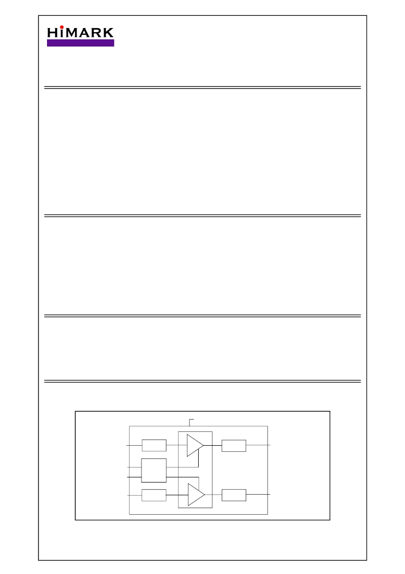
Block Diagram
the wireless IC company
GSM_IN
CMOS
Current
Buffer
Power Control
DCS_IN
Match
Match
Match
Match
HBT
Band Select
DCS_OUTPUT
GSM_OUTPUT
VCC
相關(guān)PDF資料 |
PDF描述 |
|---|---|
| PA2110 | DCS/PCS/EGSM |
| PA3-1 | Analog IC |
| PA30 | Voltage-Feedback Operational Amplifier |
| PA38-2 | 200 TO 2600 MHz CASCADABLE AMPLIFIER |
| PA44WPF | KLEMMLEISTE KABELSCHUTZ 12POL 380VAC 16A |
相關(guān)代理商/技術(shù)參數(shù) |
參數(shù)描述 |
|---|---|
| PA2100/1 | 制造商:Carlo Gavazzi 功能描述:CONTACT BLOCK 1NO SNAP ACTION |
| PA2100/2 | 制造商:Carlo Gavazzi 功能描述:Switch, Contact Block, 1-NO Contact (SPST), Slow Action, 10A @ 250VAC 制造商:Carlo Gavazzi 功能描述:CONTACT BLOCK 1NO SLOW ACTION |
| PA2101 | 制造商:Paladin Tools 功能描述: |
| PA2102 | 制造商:Paladin Tools 功能描述: |
| PA2106 | 制造商:Paladin Tools 功能描述: |
發(fā)布緊急采購(gòu),3分鐘左右您將得到回復(fù)。