- 您現(xiàn)在的位置:買賣IC網(wǎng) > PDF目錄299581 > ORLI10G-3BM416 (LATTICE SEMICONDUCTOR CORP) FPGA, 1296 CLBS, 380000 GATES, PBGA416 PDF資料下載
參數(shù)資料
| 型號(hào): | ORLI10G-3BM416 |
| 廠商: | LATTICE SEMICONDUCTOR CORP |
| 元件分類: | FPGA |
| 英文描述: | FPGA, 1296 CLBS, 380000 GATES, PBGA416 |
| 封裝: | PLASTIC, BGA-416 |
| 文件頁數(shù): | 33/76頁 |
| 文件大小: | 1222K |
| 代理商: | ORLI10G-3BM416 |
第1頁第2頁第3頁第4頁第5頁第6頁第7頁第8頁第9頁第10頁第11頁第12頁第13頁第14頁第15頁第16頁第17頁第18頁第19頁第20頁第21頁第22頁第23頁第24頁第25頁第26頁第27頁第28頁第29頁第30頁第31頁第32頁當(dāng)前第33頁第34頁第35頁第36頁第37頁第38頁第39頁第40頁第41頁第42頁第43頁第44頁第45頁第46頁第47頁第48頁第49頁第50頁第51頁第52頁第53頁第54頁第55頁第56頁第57頁第58頁第59頁第60頁第61頁第62頁第63頁第64頁第65頁第66頁第67頁第68頁第69頁第70頁第71頁第72頁第73頁第74頁第75頁第76頁
Lattice Semiconductor
39
Data Sheet
January 15, 2002
and ORLI12G Gbits/s Line Interface FPSC
ORCA ORLI10G Quad 2.5 Gbits/s, 10 Gbits/s
Timing Characteristics (continued)
Transmit STS-48/STS-192 (2.5G/10G) Data Outputs
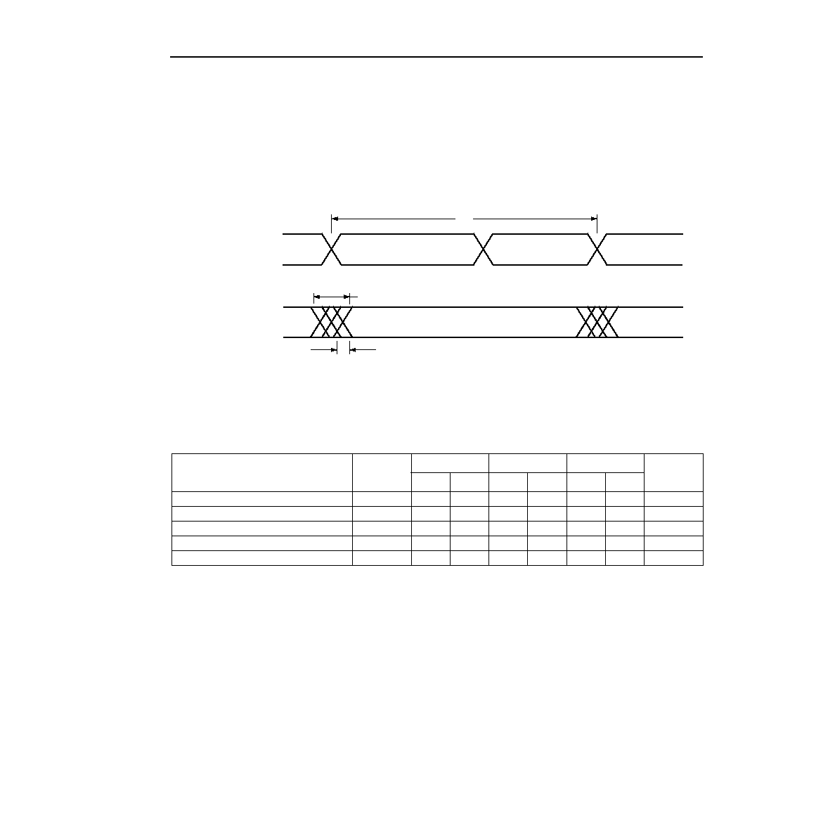
Figure 19 illustrates the timing for the transmit STS-48/STS-192 data stream. Both the clock and data pins are
driven with low-voltage differential signal (LVDS) output buffers. The expected clock rate is 622 MHz-850 MHz and
the transmit data is clocked out on the rising edge of the clock. In 2.5G mode, each of the four channels uses one
set of TX_CLK_OUTn with four TX_DAT_OUTn data pins. In 10G mode, only TX_CLK_OUT[0] is used with the
5-9089.c(F)
Figure 19. Transmit Output Data Timing
Table 14. Transmit Data Output Timing
Note: This requirement is for all sources of the output clocks (e.g., RCLKSI, etc.).
It is recommended that the Tx clock be inverted by crossing the LVDS pin pair, that is, connect the
TX_CLK_OUT_P[3:0] output on the ORLI10G to the N (i.e., complement) clock input on the receiving device and
connect the TX_CLK_OUT_N[3:0] output on the ORLI10G to the P (i.e., true) clock input on the receiving device.
This is because the receiving device that will be driven by the ORLI10G typically requires that data be centered
around the clock, but the ORLI10G drives both the clock and data from the same clock edge.
Parameter
Symbol
–1
–2
–3
Unit
Min
Max
Min
Max
Min
Max
Clock Frequency
t4
—
667
—
790
—
850
MHz
Duty Cycle
—
45
55
45
55
45
55
%
Data Delay from Clock Edge
t5
–300
300
–225
225
–210
210
ps
Data Rise Time: 20%—80%
t6
100
200
100
200
100
200
ps
Data Fall Time: 80%—20%
t7
100
200
100
200
100
200
ps
t5
TX_DAT_OUT_P[15:0]
t6
t7
TX_CLK_OUT_N[3:0]
t4
TX_CLK_OUT_P[3:0]
TX_DAT_OUT_N[15:0]
相關(guān)PDF資料 |
PDF描述 |
|---|---|
| ORLI10G-3BM680 | FPGA, 1296 CLBS, 380000 GATES, PBGA680 |
| ORLI10G1BM680-DB | FPGA, 1296 CLBS, 333000 GATES, PBGA680 |
| ORLI10G2BM680-DB | FPGA, 1296 CLBS, 333000 GATES, PBGA680 |
| ORLI10G3BM680-DB | FPGA, 1296 CLBS, 333000 GATES, PBGA680 |
| ORT82G5-1BM680 | FPGA, 1296 CLBS, 380000 GATES, PBGA680 |
相關(guān)代理商/技術(shù)參數(shù) |
參數(shù)描述 |
|---|---|
| ORLI10G-3BM680C | 功能描述:FPGA - 現(xiàn)場(chǎng)可編程門陣列 10368 LUT 316 I/O RoHS:否 制造商:Altera Corporation 系列:Cyclone V E 柵極數(shù)量: 邏輯塊數(shù)量:943 內(nèi)嵌式塊RAM - EBR:1956 kbit 輸入/輸出端數(shù)量:128 最大工作頻率:800 MHz 工作電源電壓:1.1 V 最大工作溫度:+ 70 C 安裝風(fēng)格:SMD/SMT 封裝 / 箱體:FBGA-256 |
| ORLI10G-3BMN680C | 功能描述:FPGA - 現(xiàn)場(chǎng)可編程門陣列 10368 LUT 316 I/O RoHS:否 制造商:Altera Corporation 系列:Cyclone V E 柵極數(shù)量: 邏輯塊數(shù)量:943 內(nèi)嵌式塊RAM - EBR:1956 kbit 輸入/輸出端數(shù)量:128 最大工作頻率:800 MHz 工作電源電壓:1.1 V 最大工作溫度:+ 70 C 安裝風(fēng)格:SMD/SMT 封裝 / 箱體:FBGA-256 |
| ORLI10G5-FPSC-EV | 功能描述:可編程邏輯 IC 開發(fā)工具 ORCA ORLI10G5 FPSC Eval Brd RoHS:否 制造商:Altera Corporation 產(chǎn)品:Development Kits 類型:FPGA 工具用于評(píng)估:5CEFA7F3 接口類型: 工作電源電壓: |
| ORM0200-03600 N-70 | 制造商:SMC Corporation of America 功能描述:O-RING |
| ORM120A110 | 制造商:Ssac 功能描述: |
發(fā)布緊急采購(gòu),3分鐘左右您將得到回復(fù)。