- 您現(xiàn)在的位置:買賣IC網(wǎng) > PDF目錄384797 > OR4E14 (Lineage Power) Field-Programmable Gate Arrays(現(xiàn)場(chǎng)可編程門陣列) PDF資料下載
參數(shù)資料
| 型號(hào): | OR4E14 |
| 廠商: | Lineage Power |
| 英文描述: | Field-Programmable Gate Arrays(現(xiàn)場(chǎng)可編程門陣列) |
| 中文描述: | 現(xiàn)場(chǎng)可編程門陣列(現(xiàn)場(chǎng)可編程門陣列) |
| 文件頁(yè)數(shù): | 32/132頁(yè) |
| 文件大小: | 2667K |
| 代理商: | OR4E14 |
第1頁(yè)第2頁(yè)第3頁(yè)第4頁(yè)第5頁(yè)第6頁(yè)第7頁(yè)第8頁(yè)第9頁(yè)第10頁(yè)第11頁(yè)第12頁(yè)第13頁(yè)第14頁(yè)第15頁(yè)第16頁(yè)第17頁(yè)第18頁(yè)第19頁(yè)第20頁(yè)第21頁(yè)第22頁(yè)第23頁(yè)第24頁(yè)第25頁(yè)第26頁(yè)第27頁(yè)第28頁(yè)第29頁(yè)第30頁(yè)第31頁(yè)當(dāng)前第32頁(yè)第33頁(yè)第34頁(yè)第35頁(yè)第36頁(yè)第37頁(yè)第38頁(yè)第39頁(yè)第40頁(yè)第41頁(yè)第42頁(yè)第43頁(yè)第44頁(yè)第45頁(yè)第46頁(yè)第47頁(yè)第48頁(yè)第49頁(yè)第50頁(yè)第51頁(yè)第52頁(yè)第53頁(yè)第54頁(yè)第55頁(yè)第56頁(yè)第57頁(yè)第58頁(yè)第59頁(yè)第60頁(yè)第61頁(yè)第62頁(yè)第63頁(yè)第64頁(yè)第65頁(yè)第66頁(yè)第67頁(yè)第68頁(yè)第69頁(yè)第70頁(yè)第71頁(yè)第72頁(yè)第73頁(yè)第74頁(yè)第75頁(yè)第76頁(yè)第77頁(yè)第78頁(yè)第79頁(yè)第80頁(yè)第81頁(yè)第82頁(yè)第83頁(yè)第84頁(yè)第85頁(yè)第86頁(yè)第87頁(yè)第88頁(yè)第89頁(yè)第90頁(yè)第91頁(yè)第92頁(yè)第93頁(yè)第94頁(yè)第95頁(yè)第96頁(yè)第97頁(yè)第98頁(yè)第99頁(yè)第100頁(yè)第101頁(yè)第102頁(yè)第103頁(yè)第104頁(yè)第105頁(yè)第106頁(yè)第107頁(yè)第108頁(yè)第109頁(yè)第110頁(yè)第111頁(yè)第112頁(yè)第113頁(yè)第114頁(yè)第115頁(yè)第116頁(yè)第117頁(yè)第118頁(yè)第119頁(yè)第120頁(yè)第121頁(yè)第122頁(yè)第123頁(yè)第124頁(yè)第125頁(yè)第126頁(yè)第127頁(yè)第128頁(yè)第129頁(yè)第130頁(yè)第131頁(yè)第132頁(yè)
32
Lucent Technologies Inc.
Preliminary Data Sheet
August 2000
ORCA Series 4 FPGAs
Programmable Input/Output Cells
(continued)
On the output side of each PIO, an output from the PLC
array can be routed to each output FF, and logic can be
associated with each I/O pad. The output logic associ-
ated with each pad allows for multiplexing of output sig-
nals and other functions of two output signals.
The output FF, in combination with output signal multi-
plexing, is particularly useful for registering address
signals to be multiplexed with data, allowing a full clock
cycle for the data to propagate to the output. The out-
put buffer signal can be inverted, and the 3-state con-
trol can be made active-high, active-low, or always
enabled. In addition, this 3-state signal can be regis-
tered or nonregistered.
The Series 4 I/O logic has been enhanced to include
modes for speed uplink and downlink capabilities.
These modes are supported through shift register logic
which divides down incoming data rates or multiplies
up outgoing data rates. This new logic block also sup-
ports high-speed DDR mode requirements where data
is clocked into and out of the I/O buffers on both edges
of the clock.
The new programmable I/O cell allows designers to
select I/Os that meet many new communication stan-
dards permitting the device to hookup directly without
any external interface translation. They support tradi-
tional FPGA standards as well as high-speed single-
ended and differential pair signaling (as shown in
Table 14). Based on a programmable, bank-oriented
I/O ring architecture, designs can be implemented
using 3.3 V, 2.5 V, 1.8 V, and 1.5 V output levels.
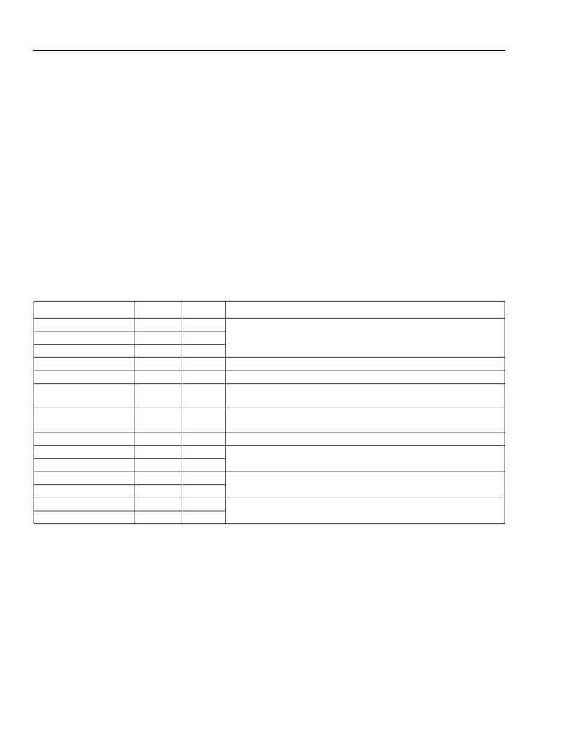
Table 14. Series 4 Programmable I/O Standards
Note: Interfaces to DDR and ZBT memories are supported through the interface standards shown above.
Standard
LVTTL
LVCMOS2
LVCMOS1.8
PCI
LVDS
Bused-LVDS
V
DDIO
(V) V
REF
(V)
3.3
2.5
1.8
3.3
2.5
2.5
Interface Usage
NA
NA
NA
NA
NA
NA
General purpose.
PCI.
Point to point and multidrop backplanes, high noise immunity.
Network backplanes, high noise immunity, bus architecture
backplanes.
Network backplanes, differential 100 MHz+ clocking, optical
transceiver, high-speed networking.
Backplanes.
Backplane or processor interface.
LVPECL
2.5
NA
PECL
GTL
GTL+
3.3
3.3
3.3
1.5
1.5
3.3
2.5
2.0
0.8
1.0
0.75
0.9
1.5
1.25
HSTL-Class I
HTSL-Class III and IV
STTL3-Class I and II
SSTL2-Class I and II
High-speed SRAM and networking interfaces.
Synchronous DRAM interface.
相關(guān)PDF資料 |
PDF描述 |
|---|---|
| OR4E2 | Field-Programmable Gate Arrays(現(xiàn)場(chǎng)可編程門陣列) |
| OR4E4 | Field-Programmable Gate Arrays(現(xiàn)場(chǎng)可編程門陣列) |
| OR4E6 | Field-Programmable Gate Arrays(現(xiàn)場(chǎng)可編程門陣列) |
| ORT4622 | Field-Programmable System Chip (FPSC) Four Channel x 622 Mbits/s Backplane Transceiver(現(xiàn)場(chǎng)可編程系統(tǒng)芯片(四通道x 622 M位/秒背板收發(fā)器)) |
| ORT8850 | Field-Programmable System Chip(現(xiàn)場(chǎng)可編程系統(tǒng)芯片) |
相關(guān)代理商/技術(shù)參數(shù) |
參數(shù)描述 |
|---|---|
| OR4E2 | 制造商:AGERE 制造商全稱:AGERE 功能描述:Field-Programmable Gate Arrays |
| OR4E2-1BA256 | 制造商:未知廠家 制造商全稱:未知廠家 功能描述:FPGA |
| OR4E2-1BA352 | 制造商:未知廠家 制造商全稱:未知廠家 功能描述:FPGA |
| OR4E2-1BA416 | 制造商:未知廠家 制造商全稱:未知廠家 功能描述:FPGA |
| OR4E2-1BC432 | 制造商:未知廠家 制造商全稱:未知廠家 功能描述:FPGA |
發(fā)布緊急采購(gòu),3分鐘左右您將得到回復(fù)。