- 您現(xiàn)在的位置:買賣IC網(wǎng) > PDF目錄299576 > OR3T165-4B600 FPGA, 1024 CLBS, 120000 GATES, PBGA600 PDF資料下載
參數(shù)資料
| 型號: | OR3T165-4B600 |
| 元件分類: | FPGA |
| 英文描述: | FPGA, 1024 CLBS, 120000 GATES, PBGA600 |
| 封裝: | BGA-600 |
| 文件頁數(shù): | 141/210頁 |
| 文件大小: | 2138K |
| 代理商: | OR3T165-4B600 |
第1頁第2頁第3頁第4頁第5頁第6頁第7頁第8頁第9頁第10頁第11頁第12頁第13頁第14頁第15頁第16頁第17頁第18頁第19頁第20頁第21頁第22頁第23頁第24頁第25頁第26頁第27頁第28頁第29頁第30頁第31頁第32頁第33頁第34頁第35頁第36頁第37頁第38頁第39頁第40頁第41頁第42頁第43頁第44頁第45頁第46頁第47頁第48頁第49頁第50頁第51頁第52頁第53頁第54頁第55頁第56頁第57頁第58頁第59頁第60頁第61頁第62頁第63頁第64頁第65頁第66頁第67頁第68頁第69頁第70頁第71頁第72頁第73頁第74頁第75頁第76頁第77頁第78頁第79頁第80頁第81頁第82頁第83頁第84頁第85頁第86頁第87頁第88頁第89頁第90頁第91頁第92頁第93頁第94頁第95頁第96頁第97頁第98頁第99頁第100頁第101頁第102頁第103頁第104頁第105頁第106頁第107頁第108頁第109頁第110頁第111頁第112頁第113頁第114頁第115頁第116頁第117頁第118頁第119頁第120頁第121頁第122頁第123頁第124頁第125頁第126頁第127頁第128頁第129頁第130頁第131頁第132頁第133頁第134頁第135頁第136頁第137頁第138頁第139頁第140頁當前第141頁第142頁第143頁第144頁第145頁第146頁第147頁第148頁第149頁第150頁第151頁第152頁第153頁第154頁第155頁第156頁第157頁第158頁第159頁第160頁第161頁第162頁第163頁第164頁第165頁第166頁第167頁第168頁第169頁第170頁第171頁第172頁第173頁第174頁第175頁第176頁第177頁第178頁第179頁第180頁第181頁第182頁第183頁第184頁第185頁第186頁第187頁第188頁第189頁第190頁第191頁第192頁第193頁第194頁第195頁第196頁第197頁第198頁第199頁第200頁第201頁第202頁第203頁第204頁第205頁第206頁第207頁第208頁第209頁第210頁
Preliminary Data Sheet, Rev. 1
ORCA Series 3 FPGAs
September 1998
36
Lucent Technologies Inc.
Programmable Input/Output Cells (continued)
Zero-Hold Input
There are two options for zero-hold input capture in the PIO. If input delay mode is selected to delay the signal from
the input pin, data can be either registered or latched with guaranteed zero-hold time in the PIO using a system
clock.
To guarantee zero hold, the system clock spine structure must be used for clocking, as will be discussed later. The
fast zero-hold mode of the PIO input takes advantage of the latch/FF combination and sources the input FF data
from a dedicated latch that is clocked by the ExpressCLK from the PIC. The ExpressCLK is a clock from a dedi-
cated input pin designed for fast, low-skew operation at the I/Os and is described more fully in the Clock Distribu-
tion Network and PIC Interquad (MID) Routing sections that follow. The combination of ExpressCLK latch and
system clock FF guarantees a zero-hold capture of input data in the PIO FF, while at the same time reducing input
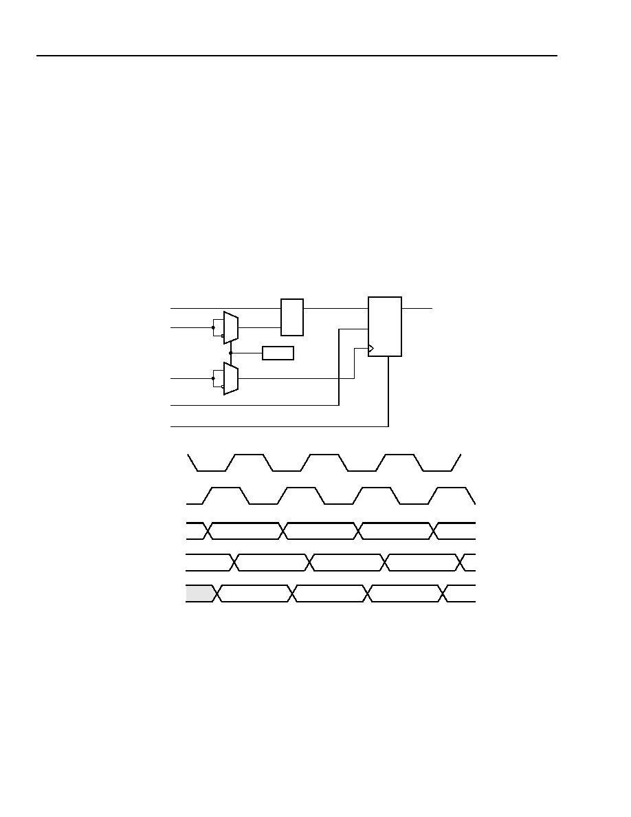
setup time. Figure 23 shows a schematic of the fast-capture latch/FF and a sample timing diagram.
5-5974(F)
Note: CE & LSR signals not shown.
Figure 23. Fast-Capture Latch and Timing
D Q
INPUT DATA
LATCH
CLK
0
1
ExpressCLK
0
1
SYSTEM CLK
CD = 1
CLOCK ENABLE
LOCAL SET/RESET
DQ
FF
S/R
CE
DATA OUT
TO PIC ROUTING
ExpressCLK
SYSTEM CLK
INPUT DATA
QLATCH
QFF
B
AC
D
E
B
AC
D
E
AB
C
D
相關(guān)PDF資料 |
PDF描述 |
|---|---|
| OR3T165-4BA352I | FPGA, 1024 CLBS, 120000 GATES, PBGA352 |
| OR3T165-4BA352 | FPGA, 1024 CLBS, 120000 GATES, PBGA352 |
| OR3T165-4BC432I | FPGA, 1024 CLBS, 120000 GATES, PBGA432 |
| OR3T165-4BC600I | FPGA, 1024 CLBS, 120000 GATES, PBGA600 |
| OR3T165-4PS208I | FPGA, 1024 CLBS, 120000 GATES, PQFP208 |
相關(guān)代理商/技術(shù)參數(shù) |
參數(shù)描述 |
|---|---|
| OR3T20 | 制造商:AGERE 制造商全稱:AGERE 功能描述:3C and 3T Field-Programmable Gate Arrays |
| OR3T20-4BA256I | 制造商:未知廠家 制造商全稱:未知廠家 功能描述:Field Programmable Gate Array (FPGA) |
| OR3T20-4S208I | 制造商:未知廠家 制造商全稱:未知廠家 功能描述:Field Programmable Gate Array (FPGA) |
| OR3T20-4S240I | 制造商:未知廠家 制造商全稱:未知廠家 功能描述:Field Programmable Gate Array (FPGA) |
| OR3T20-5BA256 | 制造商:AGERE 制造商全稱:AGERE 功能描述:3C and 3T Field-Programmable Gate Arrays |
發(fā)布緊急采購,3分鐘左右您將得到回復。