- 您現(xiàn)在的位置:買賣IC網(wǎng) > PDF目錄383714 > OR2T04A-6BC144I (Electronic Theatre Controls, Inc.) Ceramic Chip Capacitors / MIL-PRF-55681; Capacitance [nom]: 1100pF; Working Voltage (Vdc)[max]: 50V; Capacitance Tolerance: +/-1%; Dielectric: Multilayer Ceramic; Temperature Coefficient: C0G (NP0); Lead Style: Surface Mount Chip; Lead Dimensions: 1206; Termination: Solder Coated SnPb; Body Dimensions: 0.125" x 0.062" x 0.051"; Container: Bag; Features: MIL-PRF-55681: R Failure Rate PDF資料下載
參數(shù)資料
| 型號(hào): | OR2T04A-6BC144I |
| 廠商: | Electronic Theatre Controls, Inc. |
| 英文描述: | Ceramic Chip Capacitors / MIL-PRF-55681; Capacitance [nom]: 1100pF; Working Voltage (Vdc)[max]: 50V; Capacitance Tolerance: +/-1%; Dielectric: Multilayer Ceramic; Temperature Coefficient: C0G (NP0); Lead Style: Surface Mount Chip; Lead Dimensions: 1206; Termination: Solder Coated SnPb; Body Dimensions: 0.125" x 0.062" x 0.051"; Container: Bag; Features: MIL-PRF-55681: R Failure Rate |
| 中文描述: | 現(xiàn)場(chǎng)可編程門陣列 |
| 文件頁(yè)數(shù): | 48/192頁(yè) |
| 文件大小: | 3148K |
| 代理商: | OR2T04A-6BC144I |
第1頁(yè)第2頁(yè)第3頁(yè)第4頁(yè)第5頁(yè)第6頁(yè)第7頁(yè)第8頁(yè)第9頁(yè)第10頁(yè)第11頁(yè)第12頁(yè)第13頁(yè)第14頁(yè)第15頁(yè)第16頁(yè)第17頁(yè)第18頁(yè)第19頁(yè)第20頁(yè)第21頁(yè)第22頁(yè)第23頁(yè)第24頁(yè)第25頁(yè)第26頁(yè)第27頁(yè)第28頁(yè)第29頁(yè)第30頁(yè)第31頁(yè)第32頁(yè)第33頁(yè)第34頁(yè)第35頁(yè)第36頁(yè)第37頁(yè)第38頁(yè)第39頁(yè)第40頁(yè)第41頁(yè)第42頁(yè)第43頁(yè)第44頁(yè)第45頁(yè)第46頁(yè)第47頁(yè)當(dāng)前第48頁(yè)第49頁(yè)第50頁(yè)第51頁(yè)第52頁(yè)第53頁(yè)第54頁(yè)第55頁(yè)第56頁(yè)第57頁(yè)第58頁(yè)第59頁(yè)第60頁(yè)第61頁(yè)第62頁(yè)第63頁(yè)第64頁(yè)第65頁(yè)第66頁(yè)第67頁(yè)第68頁(yè)第69頁(yè)第70頁(yè)第71頁(yè)第72頁(yè)第73頁(yè)第74頁(yè)第75頁(yè)第76頁(yè)第77頁(yè)第78頁(yè)第79頁(yè)第80頁(yè)第81頁(yè)第82頁(yè)第83頁(yè)第84頁(yè)第85頁(yè)第86頁(yè)第87頁(yè)第88頁(yè)第89頁(yè)第90頁(yè)第91頁(yè)第92頁(yè)第93頁(yè)第94頁(yè)第95頁(yè)第96頁(yè)第97頁(yè)第98頁(yè)第99頁(yè)第100頁(yè)第101頁(yè)第102頁(yè)第103頁(yè)第104頁(yè)第105頁(yè)第106頁(yè)第107頁(yè)第108頁(yè)第109頁(yè)第110頁(yè)第111頁(yè)第112頁(yè)第113頁(yè)第114頁(yè)第115頁(yè)第116頁(yè)第117頁(yè)第118頁(yè)第119頁(yè)第120頁(yè)第121頁(yè)第122頁(yè)第123頁(yè)第124頁(yè)第125頁(yè)第126頁(yè)第127頁(yè)第128頁(yè)第129頁(yè)第130頁(yè)第131頁(yè)第132頁(yè)第133頁(yè)第134頁(yè)第135頁(yè)第136頁(yè)第137頁(yè)第138頁(yè)第139頁(yè)第140頁(yè)第141頁(yè)第142頁(yè)第143頁(yè)第144頁(yè)第145頁(yè)第146頁(yè)第147頁(yè)第148頁(yè)第149頁(yè)第150頁(yè)第151頁(yè)第152頁(yè)第153頁(yè)第154頁(yè)第155頁(yè)第156頁(yè)第157頁(yè)第158頁(yè)第159頁(yè)第160頁(yè)第161頁(yè)第162頁(yè)第163頁(yè)第164頁(yè)第165頁(yè)第166頁(yè)第167頁(yè)第168頁(yè)第169頁(yè)第170頁(yè)第171頁(yè)第172頁(yè)第173頁(yè)第174頁(yè)第175頁(yè)第176頁(yè)第177頁(yè)第178頁(yè)第179頁(yè)第180頁(yè)第181頁(yè)第182頁(yè)第183頁(yè)第184頁(yè)第185頁(yè)第186頁(yè)第187頁(yè)第188頁(yè)第189頁(yè)第190頁(yè)第191頁(yè)第192頁(yè)
48
Lucent Technologies Inc.
Data Sheet
June 1999
ORCA Series 2 FPGAs
FPGA Configuration Modes
(continued)
Master Serial Mode
In the master serial mode, the FPGA loads the configu-
ration data from an external serial ROM. The configura-
tion data is either loaded automatically at start-up or on
a
PRGM
command to reconfigure. The ATT1700 and
ATT1700A Series can be used to configure the FPGA
in the master serial mode. This provides a simple 4-pin
interface in an 8-pin package. The ATT1736, ATT1765,
and ATT17128 serial ROMs store 32K, 64K, and 128K
bits, respectively.
Configuration in the master serial mode can be done at
powerup and/or upon a configure command. The sys-
tem or the FPGA must activate the serial ROM's
RESET
/OE and
CE
inputs. At powerup, the FPGA and
serial ROM each contain internal power-on reset cir-
cuitry that allows the FPGA to be configured without
the system providing an external signal. The power-on
reset circuitry causes the serial ROM's internal address
pointer to be reset. After powerup, the FPGA automati-
cally enters its initialization phase.
The serial ROM/FPGA interface used depends on such
factors as the availability of a system reset pulse, avail-
ability of an intelligent host to generate a configure
command, whether a single serial ROM is used or mul-
tiple serial ROMs are cascaded, whether the serial
ROM contains a single or multiple configuration pro-
grams, etc. Because of differing system requirements
and capabilities, a single FPGA/serial ROM interface is
generally not appropriate for all applications.
Data is read in the FPGA sequentially from the serial
ROM. The DATA output from the serial ROM is con-
nected directly into the DIN input of the FPGA. The
CCLK output from the FPGA is connected to the
CLOCK input of the serial ROM. During the configura-
tion process, CCLK clocks one data bit on each rising
edge.
Since the data and clock are direct connects, the
FPGA/serial ROM design task is to use the system or
FPGA to enable the
RESET
/OE and
CE
of the serial
ROM(s). There are several methods for enabling the
serial ROM’s
RESET
/OE and
CE
inputs. The serial
ROM's
RESET
/OE is programmable to function with
RESET active-high and
OE
active-low or
RESET
active-
low and OE active-high.
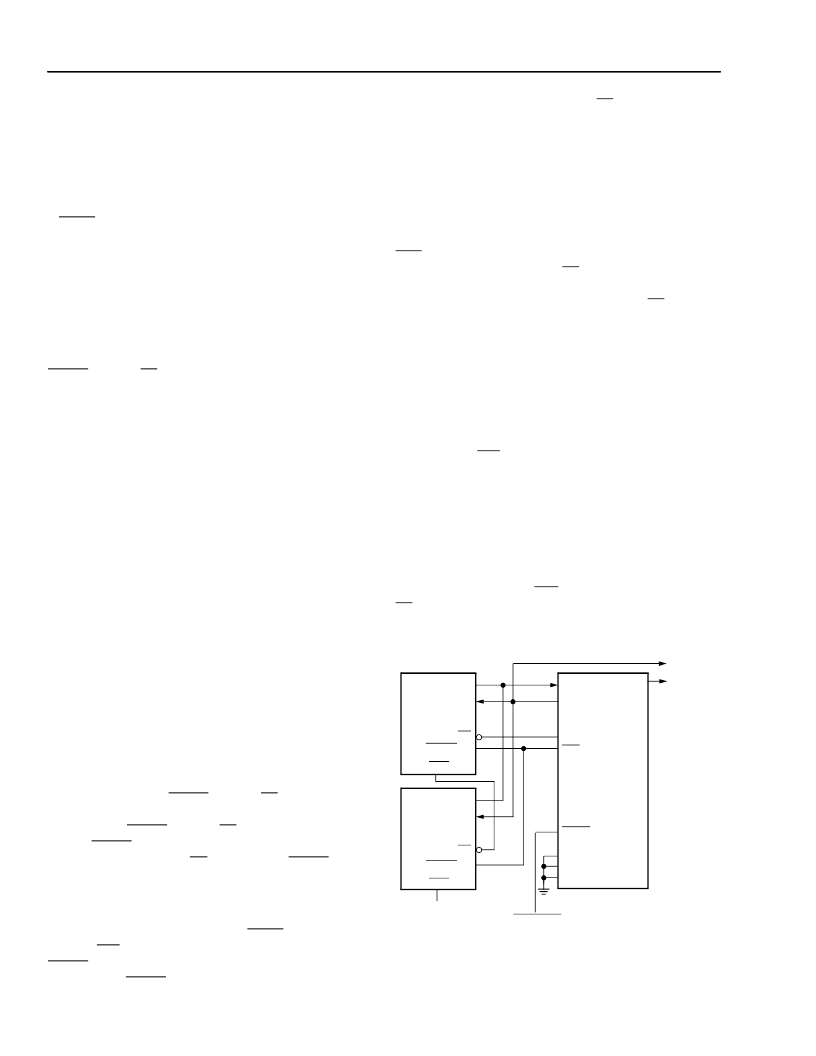
In Figure 41, serial ROMs are cascaded to configure
multiple daisy-chained FPGAs. The host generates a
500 ns low pulse into the FPGA's
PRGM
input. The
FPGA’s
INIT
input is connected to the serial ROM’s
RESET
/OE input, which has been programmed to
function with
RESET
active-low and OE active-high.
The FPGA DONE is routed to the
CE
pin. The low on
DONE enables the serial ROMs. At the completion of
configuration, the high on the FPGA's DONE disables
the serial ROM.
Serial ROMs can also be cascaded to support the con-
figuration of multiple FPGAs or to load a single FPGA
when configuration data requirements exceed the
capacity of a single serial ROM. After the last bit from
the first serial ROM is read, the serial ROM outputs
CEO
low and 3-states the DATA output. The next serial
ROM recognizes the low on
CE
input and outputs con-
figuration data on the DATA output. After configuration
is complete, the FPGA’s DONE output into
CE
disables
the serial ROMs.
This FPGA/serial ROM interface is not used in applica-
tions in which a serial ROM stores multiple configura-
tion programs. In these applications, the next
configuration program to be loaded is stored at the
ROM location that follows the last address for the previ-
ous configuration program. The reason the interface in
Figure 41 will not work in this application is that the low
output on the
INIT
signal would reset the serial ROM
address pointer, causing the first configuration to be
reloaded.
In some applications, there can be contention on the
FPGA's DIN pin. During configuration, DIN receives
configuration data, and after configuration, it is a user
I/O. If there is contention, an early DONE at start-up
(selected in ORCA Foundry) may correct the problem.
An alternative is to use
LDC
to drive the serial ROM's
CE
pin. In order to reduce noise, it is generally better to
run the master serial configuration at 1.25 MHz (M3 pin
tied high), rather than 10 MHz, if possible.
Figure 41. Master Serial Configuration Schematic
ATT1700A
DIN
M2
M1
M0
ORCA
SERIES
FPGA
CCLK
DOUT
TO DAISY-
CHAINED
DEVICES
DATA
CLK
CE
CEO
ATT1700A
DATA
CLK
RESET/OE
CEO
CE
TO MORE
SERIAL ROMs
AS NEEDED
DONE
INIT
PROGRAM
RESET/OE
PRGM
5-4456.1(F)
相關(guān)PDF資料 |
PDF描述 |
|---|---|
| OR2T04A-6BC160 | Field-Programmable Gate Arrays |
| OR2T04A-6BC160I | Field-Programmable Gate Arrays |
| OR2T04A-6S208 | Field-Programmable Gate Arrays |
| OR2T04A-6S208I | Field-Programmable Gate Arrays |
| OR2T04A-6S84 | Field-Programmable Gate Arrays |
相關(guān)代理商/技術(shù)參數(shù) |
參數(shù)描述 |
|---|---|
| OR2T04A-6BC160 | 制造商:未知廠家 制造商全稱:未知廠家 功能描述:Field-Programmable Gate Arrays |
| OR2T04A-6BC160I | 制造商:未知廠家 制造商全稱:未知廠家 功能描述:Field-Programmable Gate Arrays |
| OR2T04A-6BC208 | 制造商:未知廠家 制造商全稱:未知廠家 功能描述:Field-Programmable Gate Arrays |
| OR2T04A-6BC208I | 制造商:未知廠家 制造商全稱:未知廠家 功能描述:Field-Programmable Gate Arrays |
| OR2T04A-6BC84 | 制造商:未知廠家 制造商全稱:未知廠家 功能描述:Field-Programmable Gate Arrays |
發(fā)布緊急采購(gòu),3分鐘左右您將得到回復(fù)。