- 您現(xiàn)在的位置:買賣IC網(wǎng) > PDF目錄383714 > OR2T04A-4BC160 (Electronic Theatre Controls, Inc.) Field-Programmable Gate Arrays PDF資料下載
參數(shù)資料
| 型號: | OR2T04A-4BC160 |
| 廠商: | Electronic Theatre Controls, Inc. |
| 元件分類: | FPGA |
| 英文描述: | Field-Programmable Gate Arrays |
| 中文描述: | 現(xiàn)場可編程門陣列 |
| 文件頁數(shù): | 16/192頁 |
| 文件大?。?/td> | 3148K |
| 代理商: | OR2T04A-4BC160 |
第1頁第2頁第3頁第4頁第5頁第6頁第7頁第8頁第9頁第10頁第11頁第12頁第13頁第14頁第15頁當(dāng)前第16頁第17頁第18頁第19頁第20頁第21頁第22頁第23頁第24頁第25頁第26頁第27頁第28頁第29頁第30頁第31頁第32頁第33頁第34頁第35頁第36頁第37頁第38頁第39頁第40頁第41頁第42頁第43頁第44頁第45頁第46頁第47頁第48頁第49頁第50頁第51頁第52頁第53頁第54頁第55頁第56頁第57頁第58頁第59頁第60頁第61頁第62頁第63頁第64頁第65頁第66頁第67頁第68頁第69頁第70頁第71頁第72頁第73頁第74頁第75頁第76頁第77頁第78頁第79頁第80頁第81頁第82頁第83頁第84頁第85頁第86頁第87頁第88頁第89頁第90頁第91頁第92頁第93頁第94頁第95頁第96頁第97頁第98頁第99頁第100頁第101頁第102頁第103頁第104頁第105頁第106頁第107頁第108頁第109頁第110頁第111頁第112頁第113頁第114頁第115頁第116頁第117頁第118頁第119頁第120頁第121頁第122頁第123頁第124頁第125頁第126頁第127頁第128頁第129頁第130頁第131頁第132頁第133頁第134頁第135頁第136頁第137頁第138頁第139頁第140頁第141頁第142頁第143頁第144頁第145頁第146頁第147頁第148頁第149頁第150頁第151頁第152頁第153頁第154頁第155頁第156頁第157頁第158頁第159頁第160頁第161頁第162頁第163頁第164頁第165頁第166頁第167頁第168頁第169頁第170頁第171頁第172頁第173頁第174頁第175頁第176頁第177頁第178頁第179頁第180頁第181頁第182頁第183頁第184頁第185頁第186頁第187頁第188頁第189頁第190頁第191頁第192頁
Data Sheet
June 1999
ORCA Series 2 FPGAs
16
Lucent Technologies Inc.
Programmable Logic Cells
(continued)
The set/reset operation of the latch/FF is controlled by
two parameters: reset mode and set/reset value. When
the global set/reset (GSRN) or local set/reset (LSR) are
inactive, the storage element operates normally as a
latch or FF. The reset mode is used to select a synchro-
nous or asynchronous LSR operation. If synchronous,
LSR is enabled only if clock enable (CE) is active. For
the Series 2 series, a new option called the LSR prior-
ity allows the synchronous LSR to have priority over the
CE input, thereby setting or resetting the FF indepen-
dent of the state of CE. The clock enable is supported
on FFs, not latches. The clock enable function is imple-
mented by using a two-input multiplexer on the FF
input, with one input being the previous state of the FF
and the other input being the new data applied to the
FF. The select of this two-input multiplexer is clock
enable (CE), which selects either the new data or the
previous state. When CE is inactive, the FF output
does not change when the clock edge arrives.
The GSRN signal is only asynchronous, and it sets/
resets all latches/FFs in the FPGA based upon the set/
reset configuration bit for each latch/FF. The set/reset
value determines whether GSRN and LSR are set or
reset inputs. The set/reset value is independent for
each latch/FF.
If the local set/reset is not needed, the latch/FF can be
configured to have a data front-end select. Two data
inputs are possible in the front-end select mode, with
the LSR signal used to select which data input is used.
The data input into each latch/FF is from the output of
its associated QLUT F[3:0] or direct from WD[3:0],
bypassing the LUT. In the front-end data select mode,
both signals are available to the latches/FFs.
For PLCs that are in the two outside rows or columns of
the array, the latch/FFs can have two inputs in addition
to the F and WD inputs mentioned above. One input is
from an I/O pad located at the PIC closest to either the
left or right of the given PLC (if the PLC is in the left two
columns or right two columns of the array). The other
input is from an I/O pad located at the closest PIC
either above or below the given PLC (if the PLC is in
the top or the bottom two rows). It should be noted that
both inputs are available for a 2 x 2 array of PLCs in
each corner of the array. For the entire array of PLCs, if
either or both of these inputs is unavailable, the latch/
FF data input can be tied to a logic 0 instead (the
default).
To speed up the interface between signals external to
the FPGA and the latches/FFs, there are direct paths
from latch/FF outputs to the I/O pads. This is done for
each PLC that is adjacent to a PIC.
The latches/FFs can be configured in three modes:
1. Local synchronous set/reset: the input into the PFU’s
LSR port is used to synchronously set or reset each
latch/FF.
2. Local asynchronous set/reset: the input into LSR
asynchronously sets or resets each latch/FF.
3. Latch/FF with front-end select: the data select signal
(actually LSR) selects the input into the latches/FFs
between the LUT output and direct data in.
For all three modes, each latch/FF can be indepen-
dently programmed as either set or reset. Each latch/
FF in the PFU is independently configured to operate
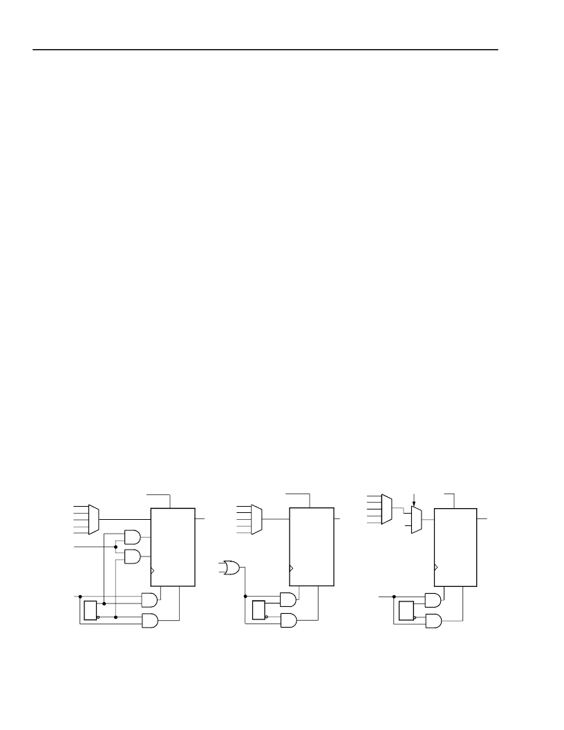
as either a latch or flip-flop. Figure 18 provides the logic
functionality of the front-end select, global set/reset,
and local set/reset operations.
Note: CD = configuration data.
5-2839(F).a
Figure 18. Latch/FF Set/Reset Configurations
CE
D
S_SET
S_RESET
CLK
SET RESET
Q
LSR
GSRN
CD
CE
D
CLK
SET RESET
LSR
CD
CE
CE
D
CLK
SET RESET
CD
CE
CE
WD
LSR
GSRN
PDINLR
LOGIC 0
WD
F
LOGIC 0
WD
GSRN
Q
Q
PDINTB
F
PDINLR
PDINTB
F
LOGIC 0
WD
PDINLR
PDINTB
相關(guān)PDF資料 |
PDF描述 |
|---|---|
| OR2T04A-4BC160I | Field-Programmable Gate Arrays |
| OR2T04A-4BC208 | Field-Programmable Gate Arrays |
| OR2T04A-4BC208I | Field-Programmable Gate Arrays |
| OR2T04A-4BC84 | Field-Programmable Gate Arrays |
| OR2T04A-4M160I | Field-Programmable Gate Arrays |
相關(guān)代理商/技術(shù)參數(shù) |
參數(shù)描述 |
|---|---|
| OR2T04A-4BC160I | 制造商:未知廠家 制造商全稱:未知廠家 功能描述:Field-Programmable Gate Arrays |
| OR2T04A-4BC208 | 制造商:未知廠家 制造商全稱:未知廠家 功能描述:Field-Programmable Gate Arrays |
| OR2T04A-4BC208I | 制造商:未知廠家 制造商全稱:未知廠家 功能描述:Field-Programmable Gate Arrays |
| OR2T04A-4BC84 | 制造商:未知廠家 制造商全稱:未知廠家 功能描述:Field-Programmable Gate Arrays |
| OR2T04A-4BC84I | 制造商:未知廠家 制造商全稱:未知廠家 功能描述:Field-Programmable Gate Arrays |
發(fā)布緊急采購,3分鐘左右您將得到回復(fù)。