- 您現(xiàn)在的位置:買賣IC網(wǎng) > PDF目錄383693 > OPA683IDR OP-AMP|SINGLE|BIPOLAR|SOP|8PIN|PLASTIC PDF資料下載
參數(shù)資料
| 型號(hào): | OPA683IDR |
| 元件分類: | 運(yùn)動(dòng)控制電子 |
| 英文描述: | OP-AMP|SINGLE|BIPOLAR|SOP|8PIN|PLASTIC |
| 中文描述: | 運(yùn)放|單|雙極|??苵 8引腳|塑料 |
| 文件頁(yè)數(shù): | 4/24頁(yè) |
| 文件大小: | 400K |
| 代理商: | OPA683IDR |
第1頁(yè)第2頁(yè)第3頁(yè)當(dāng)前第4頁(yè)第5頁(yè)第6頁(yè)第7頁(yè)第8頁(yè)第9頁(yè)第10頁(yè)第11頁(yè)第12頁(yè)第13頁(yè)第14頁(yè)第15頁(yè)第16頁(yè)第17頁(yè)第18頁(yè)第19頁(yè)第20頁(yè)第21頁(yè)第22頁(yè)第23頁(yè)第24頁(yè)
OPA683
SBOS221B
4
www.ti.com
AC PERFORMANCE (See Figure 3)
Small-Signal Bandwidth (V
O
= 0.2Vp-p)
G = +1, R
F
= 1.4k
G = +2, R
F
= 1.4k
G = +5, R
F
= 1.4k
G = +10, R
F
= 1.4k
G = +20, R
= 1.4k
G = +2, V
< 0.5Vp-p, R
= 1.2k
R
F
= 1.4k
, V
< 0.5Vp-p
G = +2, V
O
= 2Vp-p
G = +2, V
O
= 2V Step
G = +2, V
O
= 0.5V Step
G = +2, V
= 2VStep
G = 2, f = 5MHz, V
O
= 2Vp-p
R
L
= 100
to V
S
/2
R
L
≥
1k
to V
S
/2
R
L
= 100
to V
S
/2
R
L
≥
1k
f > 1MHz
f > 1MHz
f > 1MHz
G = +2, NTSC, V
O
= 1.4Vp, R
L
= 150
G = +2, NTSC, V
O
= 1.4Vp, R
L
= 150
145
119
95
87
60
14
1
70
210
5.9
7.8
MHz
MHz
MHz
MHz
MHz
MHz
dB
MHz
V/
μ
s
ns
ns
typ
min
typ
typ
typ
min
max
typ
min
typ
typ
96
92
90
B
C
C
C
B
B
C
B
C
C
Bandwidth for 0.1dB Gain Flatness
Peaking at a Gain of +1
Large-Signal Bandwidth
Slew Rate
Rise-and-Fall Time
9
6
8
8
8
8
180
175
170
Harmonic Distortion
2nd-Harmonic
–
60
–
66
–
59
–
63
4.4
5.1
11.6
0.24
0.19
–
54
–
55
–
58
–
57
5.0
5.8
11.9
–
53
–
55
–
58
–
56
5.5
6.4
12.3
–
53
–
55
–
58
–
56
5.8
6.7
12.4
dBc
dBc
dBc
dBc
nV/
√
Hz
pA/
√
Hz
pA/
√
Hz
%
deg
max
max
max
max
max
max
max
typ
typ
B
B
B
B
B
B
B
C
C
3rd-Harmonic
to V
S
/2
Input Voltage Noise
Noninverting Input Current Noise
Inverting Input Current Noise
Differential Gain
Differential Phase
DC PERFORMANCE
(4)
Open-Loop Transimpedance Gain (Z
OL
)
Input Offset Voltage
Average Offset Voltage Drift
Noninverting Input Bias Current
Average Noninverting Input Bias Current Drift
Inverting Input Bias Current
Average Inverting Input Bias Current Drift
V
O
= V
S
/2, R
= 1k
to V
S
/2
V
CM
= V
S
/2
V
CM
= V
S
/2
V
CM
= V
S
/2
V
CM
= V
S
/2
V
CM
= V
S
/2
V
CM
= V
S
/2
700
±
1.0
300
±
3.0
270
±
3.6
±
12
±
4.6
±
12
±
8.7
±
15
250
±
3.8
±
12
±
4.8
±
12
±
8.9
±
15
k
mV
μ
V/
°
C
μ
A
nA/
°
C
μ
A
nA
°
/C
min
max
max
max
max
max
max
A
A
B
A
B
A
B
±
2
±
4
±
3
±
8
INPUT
Least Positive Input Voltage
(5)
Most Positive Input Voltage
(5)
Common-Mode Refection Ratio (CMRR)
Noninverting Input Impedance
Inverting Input Resistance (R
I
)
OUTPUT
Most Positive Output Voltage
Least Positive Output Voltage
Current Output, Sourcing
Current Output, Sinking
Closed-Loop Output Impedance
1.1
3.9
58
50
2
4.8
1.25
3.75
51
1.29
3.73
50
1.34
3.67
50
V
V
dB
max
min
min
typ
typ
A
A
A
C
C
V
CM
= V
S
/2
k
|| pF
Open-Loop
R
L
= 1k
to V
S
/2
R
L
= 1k
to V
S
/2
V
O
= V
S
/2
V
= V
/2
G = +2, f = 100kHz
4.2
0.8
80
70
0.009
4.1
0.9
65
52
4.1
0.9
63
50
4.0
1.00
58
45
V
min
min
min
min
typ
A
A
A
A
C
mA
mA
DISABLE (Disabled LOW)
Power-Down Supply Current (+V
S
)
Off Isolation
Output Capacitance in Disable
Turn On Glitch
Turn Off Glitch
Enable Voltage
Disable Voltage
Control Pin Input Bias Current (DIS)
V
= 0
G = +2, 5MHz
100
70
1.7
±
70
±
20
3.4
1.8
80
μ
A
dB
pF
mV
mV
V
V
μ
A
typ
typ
typ
typ
typ
min
max
max
C
C
C
C
C
A
A
A
G = +2, R
L
= 150
, V
IN
= V
S
/2
G = +2, R
L
= 150
, V
IN
= V
S
/2
3.5
1.7
120
3.6
1.6
130
3.7
1.5
135
V
DIS
= 0V
POWER SUPPLY
Specified Single-Supply Operating Voltage
Max Single-Supply Operating Voltage
Max Quiescent Current
Min Quiescent Current
Power-Supply Rejection Ratio (+PSRR)
5
V
V
typ
max
max
min
typ
C
A
A
A
C
12
0.91
0.71
12
0.91
0.69
12
0.91
0.67
V
S
= +5V
V
= +5V
Input Referred
0.82
0.82
65
mA
mA
dB
TEMPERATURE RANGE
Specification: D, DBV
Thermal Resistance,
θ
JA
D
SO-8
DBV SOT-23-6
–
40 to +85
°
C
typ
C
Junction-to-Ambient
125
150
°
C/W
°
C/W
typ
typ
C
C
NOTES: (1) Junction temperature = ambient for 25
°
C tested specifications. (2) Junction temperature = ambient at low temperature limit: junction temperature = ambient
+2
°
C at high temperature limit for over temperature tested specifications. (3) Test levels: (A) 100% tested at 25
°
C. Over temperature limits by characterization and
simulation. (B) Limits set by characterization and simulation. (C) Typical value only for information. (4) Current is considered positive out-of-node. V
CM
is the input
common-mode voltage. (5) Tested < 3dB below minimum specified CMR at
±
CMIR limits.
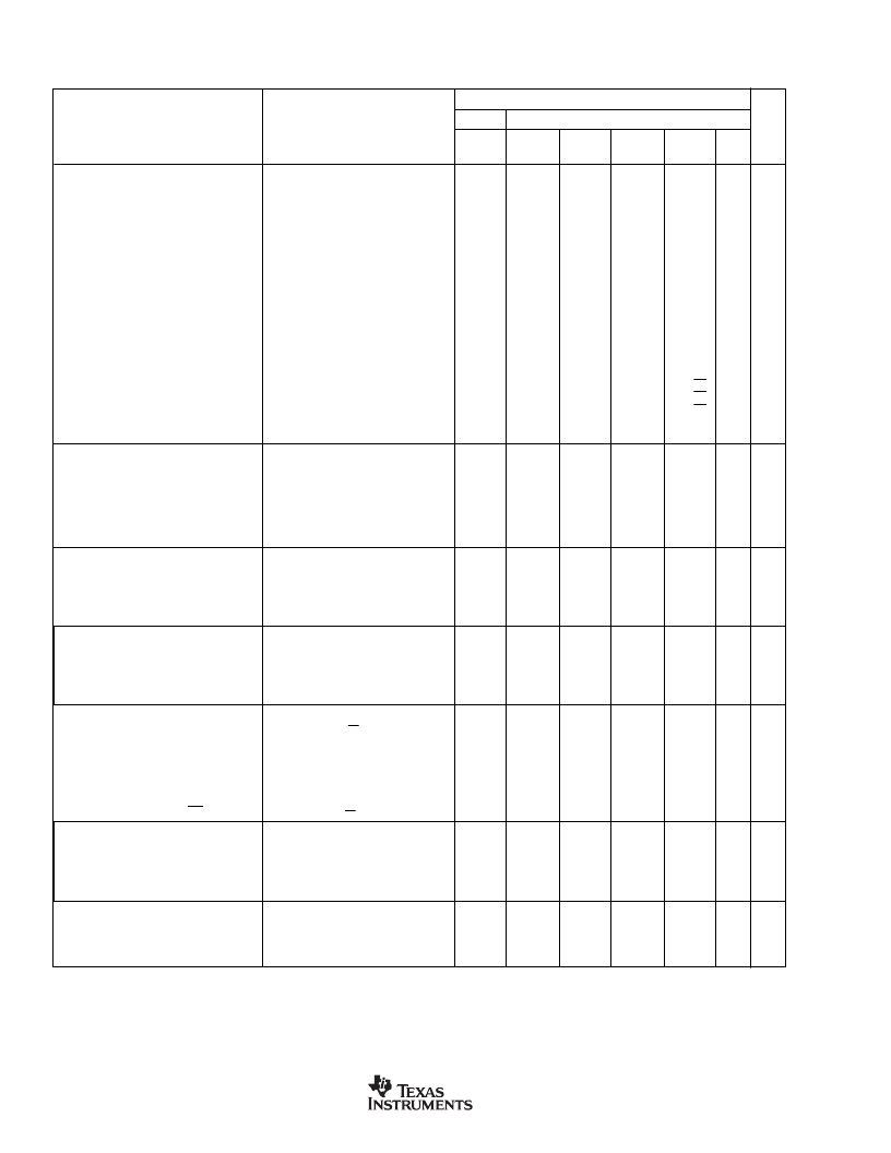
ELECTRICAL CHARACTERISTICS: V
S
= +5V
R
F
= 1.4k
, R
L
= 1k
, and G = +2
,
(see Figure 3 for AC performance only), unless otherwise noted.
OPA683ID, IDBV
TYP
MIN/MAX OVER TEMPERATURE
0
°
C to
70
°
C
(2)
–
40
°
C to
+85
°
C
(2)
MIN/
MAX
TEST
LEVEL
(3)
PARAMETER
CONDITIONS
+25
°
C
+25
°
C
(1)
UNITS
相關(guān)PDF資料 |
PDF描述 |
|---|---|
| OPA685 | Ultra-Wideband, Current-Feedback OPERATIONAL AMPLIFIER With Disable TM |
| OPA685N | Ultra-Wideband, Current-Feedback OPERATIONAL AMPLIFIER With Disable TM |
| OPA685U | Ultra-Wideband, Current-Feedback OPERATIONAL AMPLIFIER With Disable TM |
| OPA699ID | Wideband, High Gain VOLTAGE LIMITING AMPLIFIER |
| OPA699 | Wideband, High Gain VOLTAGE LIMITING AMPLIFIER |
相關(guān)代理商/技術(shù)參數(shù) |
參數(shù)描述 |
|---|---|
| OPA683IDRG4 | 功能描述:高速運(yùn)算放大器 Very Lo-Pwr Current Feedback RoHS:否 制造商:Texas Instruments 通道數(shù)量:1 電壓增益 dB:116 dB 輸入補(bǔ)償電壓:0.5 mV 轉(zhuǎn)換速度:55 V/us 工作電源電壓:36 V 電源電流:7.5 mA 最大工作溫度:+ 85 C 安裝風(fēng)格:SMD/SMT 封裝 / 箱體:SOIC-8 封裝:Tube |
| OPA684 | 制造商:BB 制造商全稱:BB 功能描述:Quad, Low-Power, Current-Feedback OPERATIONAL AMPLIFIER |
| OPA684ID | 功能描述:高速運(yùn)算放大器 Low-Power Current Feedback RoHS:否 制造商:Texas Instruments 通道數(shù)量:1 電壓增益 dB:116 dB 輸入補(bǔ)償電壓:0.5 mV 轉(zhuǎn)換速度:55 V/us 工作電源電壓:36 V 電源電流:7.5 mA 最大工作溫度:+ 85 C 安裝風(fēng)格:SMD/SMT 封裝 / 箱體:SOIC-8 封裝:Tube |
| OPA684IDBVR | 功能描述:高速運(yùn)算放大器 Low-Power Current Feedback RoHS:否 制造商:Texas Instruments 通道數(shù)量:1 電壓增益 dB:116 dB 輸入補(bǔ)償電壓:0.5 mV 轉(zhuǎn)換速度:55 V/us 工作電源電壓:36 V 電源電流:7.5 mA 最大工作溫度:+ 85 C 安裝風(fēng)格:SMD/SMT 封裝 / 箱體:SOIC-8 封裝:Tube |
| OPA684IDBVRG4 | 功能描述:高速運(yùn)算放大器 Low-Power Current Feedback RoHS:否 制造商:Texas Instruments 通道數(shù)量:1 電壓增益 dB:116 dB 輸入補(bǔ)償電壓:0.5 mV 轉(zhuǎn)換速度:55 V/us 工作電源電壓:36 V 電源電流:7.5 mA 最大工作溫度:+ 85 C 安裝風(fēng)格:SMD/SMT 封裝 / 箱體:SOIC-8 封裝:Tube |
發(fā)布緊急采購(gòu),3分鐘左右您將得到回復(fù)。