- 您現(xiàn)在的位置:買賣IC網(wǎng) > PDF目錄383693 > OPA683IDBVT OP-AMP|SINGLE|BIPOLAR|TSOP|6PIN|PLASTIC PDF資料下載
參數(shù)資料
| 型號: | OPA683IDBVT |
| 元件分類: | 運(yùn)動控制電子 |
| 英文描述: | OP-AMP|SINGLE|BIPOLAR|TSOP|6PIN|PLASTIC |
| 中文描述: | 運(yùn)放|單|雙極|的TSOP | 6針|塑料 |
| 文件頁數(shù): | 19/24頁 |
| 文件大小: | 400K |
| 代理商: | OPA683IDBVT |
OPA683
SBOS221B
19
www.ti.com
the two input bias currents, gives a worst case output offset
range equal to:
±
(NG
V
OS(MAX)
)
±
(I
BN
R
S
/2
NG)
±
(I
BI
R
F
)
where
NG = noninverting signal gain
=
±
(2
3.5mV)
±
(4
μ
A
25
2)
±
(1.2k
10
μ
A)
=
±
7mV
±
0.1mV
±
12mV
=
±
19.1mV
While the last term, the inverting bias current error, is dominant
in this low-gain circuit, the input offset voltage will become the
dominant DC error term as the gain exceeds 4V/V. Where
improved DC precision is required in a high-speed amplifier,
consider the OPA642 single and OPA2822 dual voltage-
feedback amplifiers.
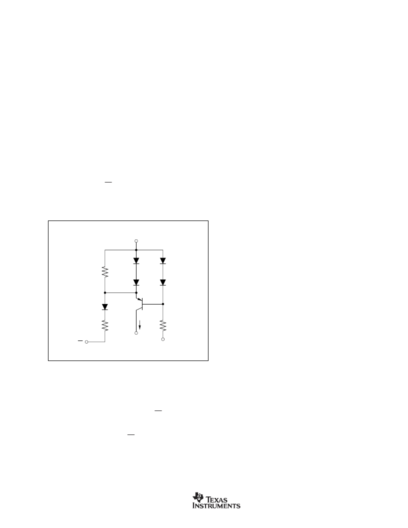
DISABLE OPERATION
The OPA683 provides an optional disable feature that may
be used to reduce system power when channel operation is
not required. If the V
DIS
control pin is left unconnected, the
OPA683 will operate normally. To disable, the control pin
must be asserted LOW. Figure 14 shows a simplified internal
circuit for the disable control feature.
In normal operation, base current to Q1 is provided through
the 250k
resistor while the emitter current through the 40k
resistor sets up a voltage drop that is inadequate to turn on
the two diodes in Q1
’
s emitter. As V
DIS
is pulled LOW,
additional current is pulled through the 40k
resistor eventu-
ally turning on these two diodes (
≈
33
μ
A). At this point, any
further current pulled out of V
DIS
goes through those diodes
holding the emitter-base voltage of Q1 at approximately 0V.
25k
250k
40k
I
Control
–
V
S
+V
S
V
DIS
Q1
FIGURE 14. Simplified Disable Control Circuit.
This shuts off the collector current out of Q1, turning the
amplifier off. The supply current in the disable mode are only
those required to operate the circuit of Figure 14.
When disabled, the output and input nodes go to a high
impedance state. If the OPA683 is operating in a gain of +1
(with a 1.2k
feedback resistor still required for stability), this
will show a very high impedance (1.7pF || 1M
) at the output
and exceptional signal isolation. If operating at a gain greater
than +1, the total feedback network resistance (R
F
+ R
G
) will
appear as the impedance looking back into the output, but
the circuit will still show very high forward and reverse
isolation. If configured as an inverting amplifier, the input and
output will be connected through the feedback network
resistance (R
F
+ R
G
) giving relatively poor input to output
isolation.
The OPA683 provides very high power gain on low quiescent
current levels. When disabled, internal high impedance nodes
discharge slowly which, with the exceptional power gain
provided, give a self powering characteristic that leads to a
slow turn off characteristic. Typical full turn off times to rated
100
μ
A disabled supply current are 60ms. Turn on times are
very fast
—
less than 40ns.
THERMAL ANALYSIS
The OPA683 will not require external heat-sinking for most
applications. Maximum desired junction temperature will set
the maximum allowed internal power dissipation as de-
scribed below. In no case should the maximum junction
temperature be allowed to exceed 175
°
C.
Operating junction temperature (T
J
) is given by T
A
+ P
D
θ
JA
.
The total internal power dissipation (P
D
) is the sum of
quiescent power (P
DQ
) and additional power dissipated in the
output stage (P
DL
) to deliver load power. Quiescent power is
simply the specified no-load supply current times the total
supply voltage across the part. P
DL
will depend on the
required output signal and load but would, for a grounded
resistive load, be at a maximum when the output is fixed at
a voltage equal to 1/2 either supply voltage (for equal bipolar
supplies). Under this condition P
DL
= V
S2
/(4
R
L
) where R
L
includes feedback network loading.
Note that it is the power in the output stage and not into the
load that determines internal power dissipation.
As an absolute worst case example, compute the maximum
T
J
using an OPA683IDBV (SOT23-6 package) in the circuit
of Figure 1 operating at the maximum specified ambient
temperature of +85
°
C and driving a grounded 100
load.
P
D
= 10V
1.05mA + 5
2
/(4
(100
|| 2.4k
)) = 76mW
Maximum T
J
= +85
°
C + (0.076W
150
°
C/W) = 96
°
C.
This maximum operating junction temperature is well below
most system level targets. Most applications will be lower
than this since an absolute worst case output stage power
was assumed in this calculation.
相關(guān)PDF資料 |
PDF描述 |
|---|---|
| OPA683IDR | OP-AMP|SINGLE|BIPOLAR|SOP|8PIN|PLASTIC |
| OPA685 | Ultra-Wideband, Current-Feedback OPERATIONAL AMPLIFIER With Disable TM |
| OPA685N | Ultra-Wideband, Current-Feedback OPERATIONAL AMPLIFIER With Disable TM |
| OPA685U | Ultra-Wideband, Current-Feedback OPERATIONAL AMPLIFIER With Disable TM |
| OPA699ID | Wideband, High Gain VOLTAGE LIMITING AMPLIFIER |
相關(guān)代理商/技術(shù)參數(shù) |
參數(shù)描述 |
|---|---|
| OPA683IDBVTG4 | 功能描述:高速運(yùn)算放大器 Very Lo-Pwr Current Feedback RoHS:否 制造商:Texas Instruments 通道數(shù)量:1 電壓增益 dB:116 dB 輸入補(bǔ)償電壓:0.5 mV 轉(zhuǎn)換速度:55 V/us 工作電源電壓:36 V 電源電流:7.5 mA 最大工作溫度:+ 85 C 安裝風(fēng)格:SMD/SMT 封裝 / 箱體:SOIC-8 封裝:Tube |
| OPA683IDG4 | 功能描述:高速運(yùn)算放大器 Very Lo-Pwr Current Feedback RoHS:否 制造商:Texas Instruments 通道數(shù)量:1 電壓增益 dB:116 dB 輸入補(bǔ)償電壓:0.5 mV 轉(zhuǎn)換速度:55 V/us 工作電源電壓:36 V 電源電流:7.5 mA 最大工作溫度:+ 85 C 安裝風(fēng)格:SMD/SMT 封裝 / 箱體:SOIC-8 封裝:Tube |
| OPA683IDR | 功能描述:高速運(yùn)算放大器 Very Lo-Pwr Current Feedback RoHS:否 制造商:Texas Instruments 通道數(shù)量:1 電壓增益 dB:116 dB 輸入補(bǔ)償電壓:0.5 mV 轉(zhuǎn)換速度:55 V/us 工作電源電壓:36 V 電源電流:7.5 mA 最大工作溫度:+ 85 C 安裝風(fēng)格:SMD/SMT 封裝 / 箱體:SOIC-8 封裝:Tube |
| OPA683IDRG4 | 功能描述:高速運(yùn)算放大器 Very Lo-Pwr Current Feedback RoHS:否 制造商:Texas Instruments 通道數(shù)量:1 電壓增益 dB:116 dB 輸入補(bǔ)償電壓:0.5 mV 轉(zhuǎn)換速度:55 V/us 工作電源電壓:36 V 電源電流:7.5 mA 最大工作溫度:+ 85 C 安裝風(fēng)格:SMD/SMT 封裝 / 箱體:SOIC-8 封裝:Tube |
| OPA684 | 制造商:BB 制造商全稱:BB 功能描述:Quad, Low-Power, Current-Feedback OPERATIONAL AMPLIFIER |
發(fā)布緊急采購,3分鐘左右您將得到回復(fù)。