- 您現(xiàn)在的位置:買賣IC網(wǎng) > PDF目錄383693 > OPA622AU OP-AMP|SINGLE|BIPOLAR|SOP|14PIN|PLASTIC PDF資料下載
參數(shù)資料
| 型號(hào): | OPA622AU |
| 英文描述: | OP-AMP|SINGLE|BIPOLAR|SOP|14PIN|PLASTIC |
| 中文描述: | 運(yùn)放|單|雙極|??苵 14PIN |塑料 |
| 文件頁數(shù): | 11/18頁 |
| 文件大小: | 335K |
| 代理商: | OPA622AU |
OPA622
11
Application circuits generally do not show the resistor
R
Q
, but it is required for proper operation.
With a fixed R
Q
, the quiescent current increases with tem-
perature (see Typical Performance Curves.) This variation
of the quiescent current with temperature keeps the band-
width and AC behavior relatively constant with temperature.
It is also possible to vary the quiescent current by an external
control signal or circuitry. Figure 3 shows a circuit to disable
the OPA622 with TTL-compatible logic levels. 0V/5V logic
levels are converted into a 1mA/0mA current connected to
Pin 2. The current flowing in R
Q
increases the voltage at Pin
2 to approximately 1V above the –V
CC
rail, thus reducing I
Q
to near zero and disabling the OPA622.
OTA AND OUTPUT BUFFER SECTIONS
An Operational Transconductance Amplifier (OTA) and an
output buffer are the basic building blocks of a current-
feedback amplifier. The current-feedback configuration of
the OPA622 is illustrated in Figure 4. The OTA consists of
a complementary emitter follower and a subsequent comple-
mentary current mirror. The voltage at the high-impedance
+In terminal is transferred to the BUF+ input/output termi-
nal at a low impedance. If a current flows into or out of the
BUF+ terminal, the complementary mirror reflects the
current to the OTA terminal. The current flow at the high-
impedance OTA terminal is determined by the product of
the voltage between the +In and BUF+ terminals and the
transconductance. The output buffer section is an open-loop
buffer consisting of complementary emitter followers. It is
designed to drive cables or low-impedance loads. The buffer
output is not current-limited or -protected. As can be seen in
Figure 4, the feedback network for a current-feedback
amplifier is applied between the V
OUT
and BUF+ terminals.
Figure 8 illustrates the bandwidth for various output volt-
ages of the current feedback configuration.
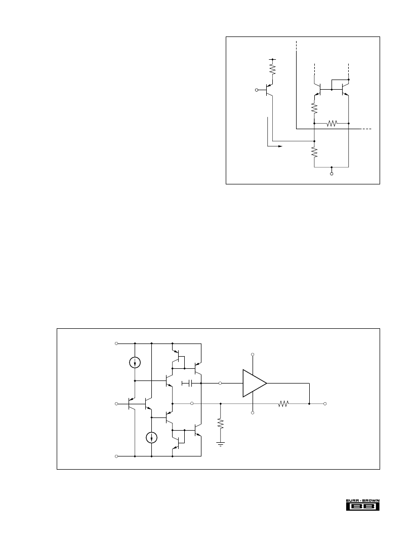
FIGURE 3. Logic-Controlled Disable Circuit.
FIGURE 4. Current-Feedback Amplifier.
100k
100
R
Q
430
–5V
Internal
Current Source
Circuitry
OPA622
2N2907
+5V
0/5V
Logic In
5V: OPA622 On
2
5
I
C
I
C
= 0: OPA622 On
I
C
= 1mA: OPA622 Off
4.7k
C
OTA
9
6
11
–V
CC OUT
V
OUT
+ V
CC OUT
R
1
R
2
10
13
12
+V
CC
5
–V
CC
+In
4
BUF+
OTA
OB
FEEDBACK BUFFER SECTION
This section of the OPA622 is a complementary emitter
follower identical to the input buffer of the OTA section. It
is designed for interstage buffering, not for driving long
cables or low-impedance loads. A minimum load resistance
of 500
is recommended when using the feedback buffer as
a stand-alone device. The feedback buffer output is not
current-limited or -protected. The bandwidth of the feedback
buffer is shown in Figure 7.
相關(guān)PDF資料 |
PDF描述 |
|---|---|
| OPA623 | Wide Bandwidth, Current-Feedback OPERATIONAL AMPLIFIER |
| OPA623AP | Wide Bandwidth, Current-Feedback OPERATIONAL AMPLIFIER |
| OPA623AU | Wide Bandwidth, Current-Feedback OPERATIONAL AMPLIFIER |
| OPA628AU | Low Distortion Wideband OPERATIONAL AMPLIFIER |
| OPA628 | Low Distortion Wideband OPERATIONAL AMPLIFIER |
相關(guān)代理商/技術(shù)參數(shù) |
參數(shù)描述 |
|---|---|
| OPA623 | 制造商:BB 制造商全稱:BB 功能描述:Wide Bandwidth, Current-Feedback OPERATIONAL AMPLIFIER |
| OPA623 WAF | 制造商:Texas Instruments 功能描述: |
| OPA623AP | 制造商:BB 制造商全稱:BB 功能描述:Wide Bandwidth, Current-Feedback OPERATIONAL AMPLIFIER |
| OPA623AU | 制造商:BB 制造商全稱:BB 功能描述:Wide Bandwidth, Current-Feedback OPERATIONAL AMPLIFIER |
| OPA6250 | 制造商:TI 制造商全稱:Texas Instruments 功能描述:Wideband, Unity-Gain Stable, FET-Input OPERATIONAL AMPLIFIER |
發(fā)布緊急采購(gòu),3分鐘左右您將得到回復(fù)。