- 您現(xiàn)在的位置:買賣IC網(wǎng) > PDF目錄383692 > OPA340NA-3K Voltage-Feedback Operational Amplifier PDF資料下載
參數(shù)資料
| 型號(hào): | OPA340NA-3K |
| 英文描述: | Voltage-Feedback Operational Amplifier |
| 中文描述: | 電壓反饋運(yùn)算放大器 |
| 文件頁數(shù): | 9/11頁 |
| 文件大小: | 255K |
| 代理商: | OPA340NA-3K |
9
OPA340/2340/4340
OPA340 series op amps are laser-trimmed to the reduce
offset voltage difference between the N-channel and
P-channel input stages, resulting in improved common-
mode rejection and a smooth transition between the
N-channel pair and the P-channel pair. However, within the
400mV transition region PSRR, CMRR, offset voltage,
offset drift, and THD may be degraded compared to opera-
tion outside this region.
A double-folded cascode adds the signal from the two input
pairs and presents a differential signal to the class AB output
stage. Normally, input bias current is approximately 200fA,
however, input voltages exceeding the power supplies by
more than 500mV can cause excessive current to flow in or
out of the input pins. Momentary voltages greater than
500mV beyond the power supply can be tolerated if the
current on the input pins is limited to 10mA. This is easily
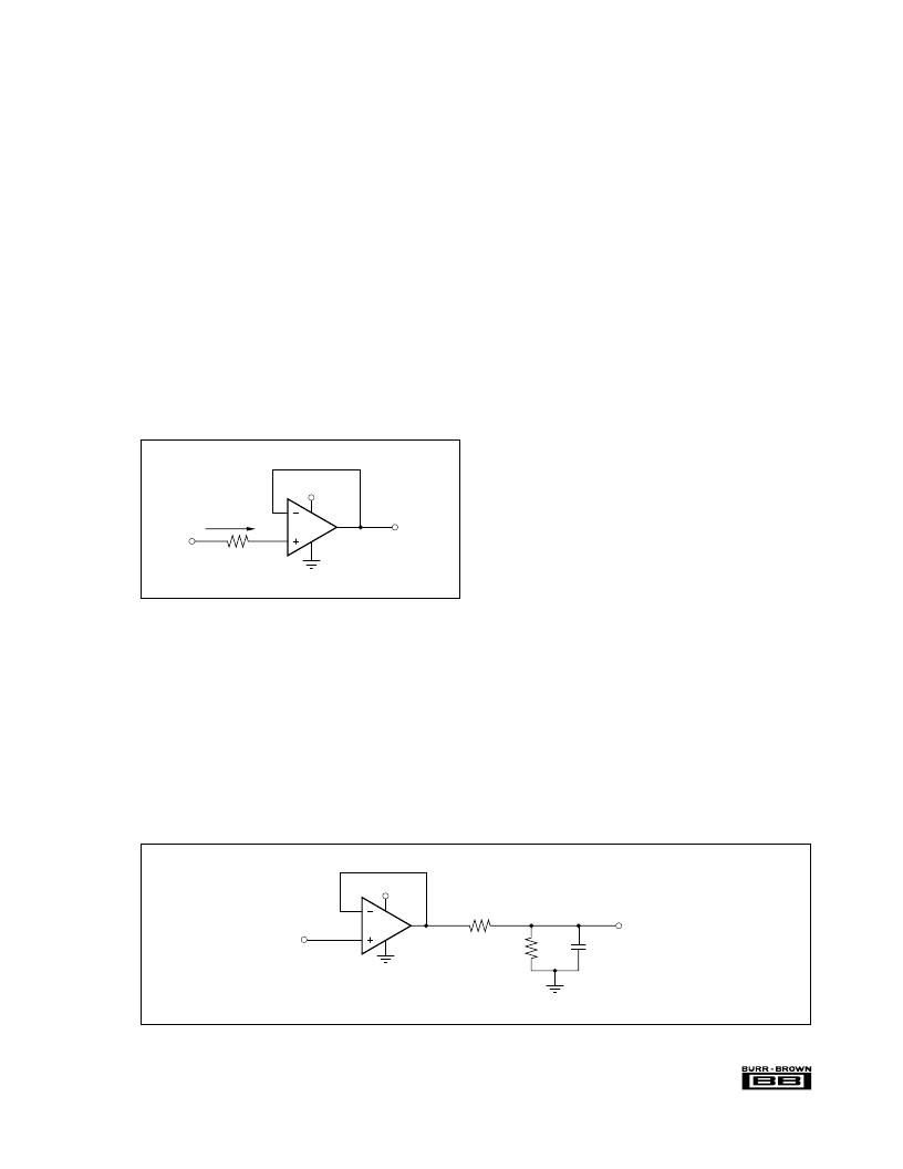
accomplished with an input resistor as shown in Figure 3.
Many input signals are inherently current-limited to less
than 10mA, therefore, a limiting resistor is not required.
CAPACITIVE LOAD AND STABILITY
OPA340 series op amps can drive a wide range of capacitive
loads. However, all op amps under certain conditions may
become unstable. Op amp configuration, gain, and load
value are just a few of the factors to consider when determin-
ing stability. An op amp in unity gain configuration is the
most susceptible to the effects of capacitive load. The
capacitive load reacts with the op amp’s output resistance,
along with any additional load resistance, to create a pole in
the small-signal response which degrades the phase margin.
In unity gain, OPA340 series op amps perform well, with a
pure capacitive load up to approximately 1000pF. Increasing
gain enhances the amplifier’s ability to drive more capaci-
tance. See the typical performance curve “Small-Signal
Overshoot vs Capacitive Load.”
One method of improving capacitive load drive in the unity
gain configuration is to insert a 10
to 20
resistor in series
with the output, as shown in Figure 4. This significantly
reduces ringing with large capacitive loads. However, if
there is a resistive load in parallel with the capacitive load,
it creates a voltage divider introducing a dc error at the
output and slightly reduces output swing. This error may be
insignificant. For instance, with R
L
= 10k
and R
S
= 20
,
there is only about a 0.2% error at the output.
DRIVING A/D CONVERTERS
OPA340 series op amps are optimized for driving medium
speed (up to 100kHz) sampling A/D converters. However,
they also offer excellent performance for higher speed
converters. The OPA340 series provides an effective means
of buffering the A/D’s input capacitance and resulting
charge injection while providing signal gain.
Figures 5 and 6 show the OPA340 driving an ADS7816.
The ADS7816 is a 12-bit, micro-power sampling converter
in the tiny MSOP-8 package. When used with the minia-
ture package options of the OPA340 series, the combina-
tion is ideal for space-limited and low power applications.
For further information consult the ADS7816 data sheet.
With the OPA340 in a noninverting configuration, an RC
network at the amplifier’s output can be used to filter high
frequency noise in the signal (Figure 5). In the inverting
configuration, filtering may be accomplished with a ca-
pacitor across the feedback resistor (Figure 6).
FIGURE 3. Input Current Protection for Voltages Exceeding
the Supply Voltage.
5k
OPAx340
10mA max
V+
V
IN
V
OUT
I
OVERLOAD
RAIL-TO-RAIL OUTPUT
A class AB output stage with common-source transistors is
used to achieve rail-to-rail output. For light resistive loads
(>50k
), the output voltage is typically a few millivolts
from the supply rails. With moderate resistive loads (2k
to
50k
), the output can swing to within a few tens of milli-
volts from the supply rails and maintain high open-loop
gain. See the typical performanc curve “Output Voltage
Swing vs Output Current.”
FIGURE 4. Series Resistor in Unity-Gain Configuration Improves Capacitive Load Drive.
10
to
20
OPAx340
V+
V
IN
V
OUT
R
S
R
L
C
L
相關(guān)PDF資料 |
PDF描述 |
|---|---|
| OPA2340EA-2500 | Voltage-Feedback Operational Amplifier |
| OPA2342 | OPA2342 - Low Cost. Low Power. Rail-to-Rail OPERATIONAL AMPLIFIERS MicroAmplifier Series |
| OPA237 | Single-Supply Operational Amplifiers MicroAmplifier(TM) Series |
| OPA4340EA-250 | Voltage-Feedback Operational Amplifier |
| OPA4340EA-2500 | Voltage-Feedback Operational Amplifier |
相關(guān)代理商/技術(shù)參數(shù) |
參數(shù)描述 |
|---|---|
| OPA340PA | 功能描述:運(yùn)算放大器 - 運(yùn)放 Single-Supply Rail-to-Rail RoHS:否 制造商:STMicroelectronics 通道數(shù)量:4 共模抑制比(最小值):63 dB 輸入補(bǔ)償電壓:1 mV 輸入偏流(最大值):10 pA 工作電源電壓:2.7 V to 5.5 V 安裝風(fēng)格:SMD/SMT 封裝 / 箱體:QFN-16 轉(zhuǎn)換速度:0.89 V/us 關(guān)閉:No 輸出電流:55 mA 最大工作溫度:+ 125 C 封裝:Reel |
| OPA340PA | 制造商:BURR-BROWN 功能描述:IC OP-AMP CMOS RRI/O |
| OPA340PAG4 | 功能描述:運(yùn)算放大器 - 運(yùn)放 Single-Supply Rail-to-Rail RoHS:否 制造商:STMicroelectronics 通道數(shù)量:4 共模抑制比(最小值):63 dB 輸入補(bǔ)償電壓:1 mV 輸入偏流(最大值):10 pA 工作電源電壓:2.7 V to 5.5 V 安裝風(fēng)格:SMD/SMT 封裝 / 箱體:QFN-16 轉(zhuǎn)換速度:0.89 V/us 關(guān)閉:No 輸出電流:55 mA 最大工作溫度:+ 125 C 封裝:Reel |
| OPA340UA | 功能描述:運(yùn)算放大器 - 運(yùn)放 SOIC-8 RoHS:否 制造商:STMicroelectronics 通道數(shù)量:4 共模抑制比(最小值):63 dB 輸入補(bǔ)償電壓:1 mV 輸入偏流(最大值):10 pA 工作電源電壓:2.7 V to 5.5 V 安裝風(fēng)格:SMD/SMT 封裝 / 箱體:QFN-16 轉(zhuǎn)換速度:0.89 V/us 關(guān)閉:No 輸出電流:55 mA 最大工作溫度:+ 125 C 封裝:Reel |
| OPA340UA | 制造商:BURR-BROWN 功能描述:OP AMP CMOS RRI/O SMD SOIC8 340 制造商:Texas Instruments 功能描述:Operational Amplifier IC Number of Ampli |
發(fā)布緊急采購,3分鐘左右您將得到回復(fù)。