- 您現(xiàn)在的位置:買賣IC網(wǎng) > PDF目錄361138 > NSTB1005DXV5T1 (ON SEMICONDUCTOR) Dual Common Base(雙通用基極-集電極偏置電阻晶體管) PDF資料下載
參數(shù)資料
| 型號: | NSTB1005DXV5T1 |
| 廠商: | ON SEMICONDUCTOR |
| 元件分類: | 小信號晶體管 |
| 英文描述: | Dual Common Base(雙通用基極-集電極偏置電阻晶體管) |
| 中文描述: | 100 mA, 50 V, 2 CHANNEL, NPN AND PNP, Si, SMALL SIGNAL TRANSISTOR |
| 封裝: | CASE 463B-01, 5 PIN |
| 文件頁數(shù): | 1/6頁 |
| 文件大?。?/td> | 59K |
| 代理商: | NSTB1005DXV5T1 |
Semiconductor Components Industries, LLC, 2004
March, 2004 Rev. 0
1
Publication Order Number:
NSTB1005DXV5/D
NSTB1005DXV5T1,
NSTB1005DXV5T5
Preferred Devices
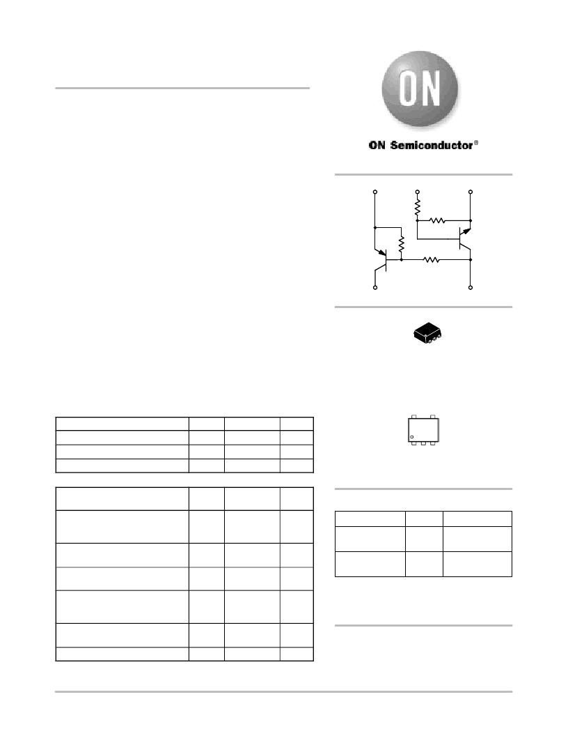
Dual Common
BaseCollector Bias
Resistor Transistors
NPN and PNP Silicon Surface Mount
Transistors with Monolithic Bias
Resistor Network
The BRT (Bias Resistor Transistor) contains a single transistor with
a monolithic bias network consisting of two resistors; a series base
resistor and a baseemitter resistor. These digital transistors are
designed to replace a single device and its external resistor bias
network. The BRT eliminates these individual components by
integrating them into a single device. The NSTB1005DXV5T1
contains two complementary BRT devices are housed in the SOT553
package which is ideal for low power surface mount applications
where board space is at a premium.
Simplifies Circuit Design
Reduces Board Space
Reduces Component Count
Available in 8 mm, 7 inch Tape and Reel
Lead Free
MAXIMUM RATINGS
(T
A
= 25
°
C unless otherwise noted, common for Q
1
and Q
2
, minus sign for Q
1
(PNP) omitted)
Rating
Symbol
Value
Unit
Collector-Base Voltage
V
CBO
50
Vdc
Collector-Emitter Voltage
V
CEO
50
Vdc
Collector Current
I
C
100
mAdc
THERMAL CHARACTERISTICS
Characteristic
(One Junction Heated)
Symbol
Max
Unit
Total Device Dissipation
T
A
= 25
°
C
Derate above 25
°
C
P
D
357 (Note 1)
2.9 (Note 1)
mW
mW/
°
C
Thermal Resistance
Junction-to-Ambient
R
JA
350 (Note 1)
°
C/W
Characteristic
(Both Junctions Heated)
Symbol
Max
Unit
Total Device Dissipation
T
A
= 25
°
C
Derate above 25
°
C
P
D
500 (Note 1)
4.0 (Note 1)
mW
mW/
°
C
Thermal Resistance
Junction-to-Ambient
R
JA
250 (Note 1)
°
C/W
Junction and Storage Temperature
T
J
, T
stg
55 to +150
°
C
1. FR4 @ Minimum Pad
MARKING DIAGRAM
Preferred
devices are recommended choices for future use
and best overall value.
4
5
Q1
Q2
R1
R1
R2
3
1
2
http://onsemi.com
SOT553
CASE 463B
UC D
1
5
1
5
UC = Specific Device Code
D
= Date Code
Device
Package
Shipping
ORDERING INFORMATION
NSTB1005DXV5T1 SOT553
4 mm pitch
4000/Tape & Reel
NSTB1005DXV5T5 SOT553
2 mm pitch
8000/Tape & Reel
R2
For information on tape and reel specifications,
including part orientation and tape sizes, please
refer to our Tape and Reel Packaging Specification
Brochure, BRD8011/D.
相關(guān)PDF資料 |
PDF描述 |
|---|---|
| NSVS784 | JRC SAW FILTER |
| NT6880 | Keyboard Controller |
| NT6880H | Keyboard Controller |
| NT68P81 | USB Keyboard Micro-Controller |
| NT68P81-D01012 | USB Keyboard Micro-Controller |
相關(guān)代理商/技術(shù)參數(shù) |
參數(shù)描述 |
|---|---|
| NSTB1005DXV5T1G | 功能描述:兩極晶體管 - BJT 100mA Complementary 50V Dual NPN & PNP RoHS:否 制造商:STMicroelectronics 配置: 晶體管極性:PNP 集電極—基極電壓 VCBO: 集電極—發(fā)射極最大電壓 VCEO:- 40 V 發(fā)射極 - 基極電壓 VEBO:- 6 V 集電極—射極飽和電壓: 最大直流電集電極電流: 增益帶寬產(chǎn)品fT: 直流集電極/Base Gain hfe Min:100 A 最大工作溫度: 安裝風格:SMD/SMT 封裝 / 箱體:PowerFLAT 2 x 2 |
| NSTB1005DXV5T5 | 功能描述:開關(guān)晶體管 - 偏壓電阻器 100mA Complementary RoHS:否 制造商:ON Semiconductor 配置: 晶體管極性:NPN/PNP 典型輸入電阻器: 典型電阻器比率: 安裝風格:SMD/SMT 封裝 / 箱體: 直流集電極/Base Gain hfe Min:200 mA 最大工作頻率: 集電極—發(fā)射極最大電壓 VCEO:50 V 集電極連續(xù)電流:150 mA 峰值直流集電極電流: 功率耗散:200 mW 最大工作溫度: 封裝:Reel |
| NSTB1005DXV5T5G | 功能描述:開關(guān)晶體管 - 偏壓電阻器 100mA Complementary 50V Dual NPN & PNP RoHS:否 制造商:ON Semiconductor 配置: 晶體管極性:NPN/PNP 典型輸入電阻器: 典型電阻器比率: 安裝風格:SMD/SMT 封裝 / 箱體: 直流集電極/Base Gain hfe Min:200 mA 最大工作頻率: 集電極—發(fā)射極最大電壓 VCEO:50 V 集電極連續(xù)電流:150 mA 峰值直流集電極電流: 功率耗散:200 mW 最大工作溫度: 封裝:Reel |
| NSTB60ADW1T1/D | 制造商:未知廠家 制造商全稱:未知廠家 功能描述:PNP General Purpose and NPN Bias Resistor Transistor Combination |
| NSTB60BDW1T1 | 功能描述:開關(guān)晶體管 - 偏壓電阻器 150mA Complementary RoHS:否 制造商:ON Semiconductor 配置: 晶體管極性:NPN/PNP 典型輸入電阻器: 典型電阻器比率: 安裝風格:SMD/SMT 封裝 / 箱體: 直流集電極/Base Gain hfe Min:200 mA 最大工作頻率: 集電極—發(fā)射極最大電壓 VCEO:50 V 集電極連續(xù)電流:150 mA 峰值直流集電極電流: 功率耗散:200 mW 最大工作溫度: 封裝:Reel |
發(fā)布緊急采購,3分鐘左右您將得到回復(fù)。