- 您現(xiàn)在的位置:買賣IC網(wǎng) > PDF目錄299557 > NM93CS46TLVM8X (FAIRCHILD SEMICONDUCTOR CORP) 64 X 16 MICROWIRE BUS SERIAL EEPROM, PDSO8 PDF資料下載
參數(shù)資料
| 型號: | NM93CS46TLVM8X |
| 廠商: | FAIRCHILD SEMICONDUCTOR CORP |
| 元件分類: | PROM |
| 英文描述: | 64 X 16 MICROWIRE BUS SERIAL EEPROM, PDSO8 |
| 封裝: | 0.150 INCH, PLASTIC, SO-8 |
| 文件頁數(shù): | 11/16頁 |
| 文件大小: | 163K |
| 代理商: | NM93CS46TLVM8X |
4
www.fairchildsemi.com
NM93CS46 Rev. F.2
NM93CS46
(MICROWIRE
Bus
Interface)
1024-Bit
Serial
EEPROM
with
Data
Protect
and
Sequential
Read
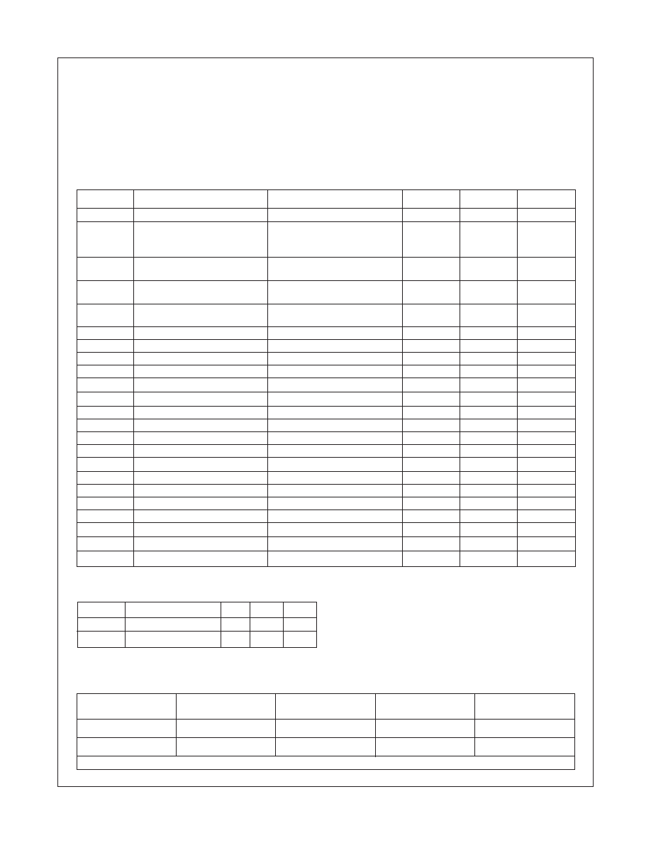
Absolute Maximum Ratings (Note 1)
Ambient Storage Temperature
-65
°C to +150°C
All Input or Output Voltages
+6.5V to -0.3V
with Respect to Ground
Lead Temperature
(Soldering, 10 sec.)
+300
°C
ESD rating
2000V
Operating Conditions
Ambient Operating Temperature
NM93CS46L/LZ
0
°C to +70°C
NM93CS46LE/LZE
-40
°C to +85°C
NM93CS46LV/LZV
-40
°C to +125°C
Power Supply (V
CC)
2.7V to 5.5V
DC and AC Electrical Characteristics V
CC = 2.7V to 5.5V unless otherwise specified
SymbolParameter
Conditions
Min
Max
Units
I
CCA
Operating Current
CS = V
IH, SK=1.0 MHz
1
mA
I
CCS
Standby Current
CS = V
IL
L
10
A
LZ (2.7V to 4.5V)
1
A
I
IL
Input Leakage
V
IN = 0V to VCC
±1
A
IOL
Output Leakage
(Note 2)
V
IL
Input Low Voltage
-0.1
0.15V
CC
V
VIH
Input High Voltage
0.8VCC
VCC +1
V
OL
Output Low Voltage
I
OL = 10A
0.1V
CC
V
OH
Output High Voltage
I
OH = -10A
0.9V
CC
f
SK
SK Clock Frequency
(Note 3)
0
250
KHz
tSKH
SK High Time
1
s
t
SKL
SK Low Time
1
s
tSKS
SK Setup Time
0.2
s
t
CS
Minimum CS Low Time
(Note 4)
1
s
t
CSS
CS Setup Time
0.2
s
tPRES
PRE Setup Time
50
ns
t
DH
DO Hold Time
70
ns
tPES
PE Setup Time
50
ns
t
DIS
DI Setup Time
0.4
s
t
CSH
CS Hold Time
0
ns
tPEH
PE Hold Time
250
ns
t
PREH
PRE Hold Time
50
ns
tDIH
DI Hold Time
0.4
s
t
PD
Output Delay
2
s
t
SV
CS to Status Valid
1
s
tDF
CS to DO in Hi-Z
CS = VIL
0.4
s
t
WP
Write Cycle Time
15
ms
Capacitance T
A = 25°C, f = 1 MHz (Note 5)
SymbolTest
Typ
Max
Units
COUT
Output Capacitance
5
pF
C
IN
Input Capacitance
5
pF
Note 1:
Stress above those listed under “Absolute Maximum Ratings” may cause permanent damage
to the device. This is a stress rating only and functional operation of the device at these or any other
conditions above those indicated in the operational sections of the specification is not implied. Exposure
to absolute maximum rating conditions for extended periods may affect device reliability.
Note 2:
Typical leakage values are in the 20nA range.
Note 3:
The shortest allowable SK clock period = 1/fSK (as shown under the fSK parameter). Maximum
SK clock speed (minimum SK period) is determined by the interaction of several AC parameters stated
in the datasheet. Within this SK period, both tSKH and tSKL limits must be observed. Therefore, it is not
allowable to set 1/fSK = tSKHminimum + tSKLminimum for shorter SK cycle time operation.
Note 4:
CS (Chip Select) must be brought low (to VIL) for an interval of tCS in order to reset all internal
device registers (device reset) prior to beginning another opcode cycle. (This is shown in the opcode
diagram on the following page.)
Note 5:
This parameter is periodically sampled and not 100% tested.
AC Test Conditions
V
CC Range
V
IL/VIH
V
IL/VIH
V
OL/VOH
I
OL/IOH
Input Levels
Timing Level
2.7V
≤ V
CC ≤ 5.5V
0.3V/1.8V
1.0V
0.8V/1.5V
±10A
(Extended Voltage Levels)
4.5V
≤ V
CC ≤ 5.5V
0.4V/2.4V
1.0V/2.0V
0.4V/2.4V
2.1mA/-0.4mA
(TTL Levels)
Output Load: 1 TTL Gate (C
L = 100 pF)
相關PDF資料 |
PDF描述 |
|---|---|
| NM93CS56LEMT8X | 128 X 16 MICROWIRE BUS SERIAL EEPROM, PDSO8 |
| NM93CS56MT8X | 128 X 16 MICROWIRE BUS SERIAL EEPROM, PDSO8 |
| NMC93C66MX | 256 X 16 MICROWIRE BUS SERIAL EEPROM, PDSO14 |
| NMXD0515U | 2-OUTPUT 5 W DC-DC REG PWR SUPPLY MODULE |
| NMXS1205U | 1-OUTPUT 5 W DC-DC REG PWR SUPPLY MODULE |
相關代理商/技術參數(shù) |
參數(shù)描述 |
|---|---|
| NM93CS46TLVMT8 | 制造商:未知廠家 制造商全稱:未知廠家 功能描述:Microwire Serial EEPROM |
| NM93CS46TLVN | 制造商:未知廠家 制造商全稱:未知廠家 功能描述:Microwire Serial EEPROM |
| NM93CS46TLZEM8 | 制造商:未知廠家 制造商全稱:未知廠家 功能描述:Microwire Serial EEPROM |
| NM93CS46TLZEMT8 | 制造商:未知廠家 制造商全稱:未知廠家 功能描述:Microwire Serial EEPROM |
| NM93CS46TLZEN | 制造商:未知廠家 制造商全稱:未知廠家 功能描述:Microwire Serial EEPROM |
發(fā)布緊急采購,3分鐘左右您將得到回復。