- 您現(xiàn)在的位置:買賣IC網(wǎng) > PDF目錄299551 > NCP1546DG (ON SEMICONDUCTOR) 1.5A 170 kHz Low Voltage Buck Regulator PDF資料下載
參數(shù)資料
| 型號: | NCP1546DG |
| 廠商: | ON SEMICONDUCTOR |
| 元件分類: | 穩(wěn)壓器 |
| 英文描述: | 1.5A 170 kHz Low Voltage Buck Regulator |
| 中文描述: | SWITCHING REGULATOR, PDSO8 |
| 封裝: | LEAD FREE, SOIC-8 |
| 文件頁數(shù): | 9/15頁 |
| 文件大小: | 212K |
| 代理商: | NCP1546DG |
NCP1546
http://onsemi.com
3
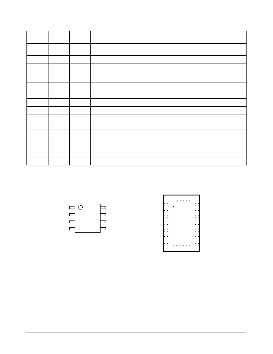
PACKAGE PIN DESCRIPTION
SO8
DFN18
PIN
SYMBOL
FUNCTION
1
BOOST
The BOOST pin provides additional drive voltage to the onchip NPN power transistor. The
resulting decrease in switch on voltage increases efficiency.
2
24
VIN
This pin is the main power input to the IC.
3
57
VSW
This is the connection to the emitter of the onchip NPN power transistor and serves as the
switch output to the inductor. This pin may be subjected to negative voltages during switch off
time. A catch diode is required to clamp the pin voltage in normal operation. This node can
stand 1.0 V for less than 50 ns during switch node flyback.
4
8
SHDNB
The shutdown pin is active low and TTL compatible. The IC goes into sleep mode, drawing less
than 1.0 mA when the pin voltage is pulled below 1.0 V.
This pin should be pulled up to VCC with a resistor.
5
10
SYNC
This pin provides the synchronization input.
6
13
GND
Power return connection for the IC.
7
16
VFB
The FB pin provides input to the inverting input of the error amplifier. If VFB is lower than 0.29 V,
the oscillator frequency is divided by four, and current limit folds back to about 1 ampere. These
features protect the IC under severe overcurrent or short circuit conditions.
8
17
VC
The VC pin provides a connection point to the output of the error amplifier and input to the PWM
comparator. Driving of this pin should be avoided because onchip test circuitry becomes active
whenever current exceeding 0.5 mA is forced into the IC.
9, 11, 12,
14, 15, 18
NC
No Connection
Exposed die attach pad. Internally connected to GND. External connection to GND is optional.
PIN CONNECTIONS
1
2
3
4
5
6
7
8
9
18
17
16
15
14
13
12
11
10
BOOST
VIN
Vsw
VSW
SHDNB
NC
VC
VFB
NC
GND
NC
SYNC
18Lead DFN
1
8
SYNC
SHDNB
GND
VSW
VFB
VIN
VC
BOOST
SO8
相關(guān)PDF資料 |
PDF描述 |
|---|---|
| NCP362BMUTBG | OVP/OCP + TVS |
| NCT1008DMT3R2G | %2B-1℃ temperature monitor with series resistance cancellation |
| NCV4275ADS50G | 450 mA, 5.0V, LDO w/Reset and Delay |
| NCV4275ADS50R4G | 450 mA, 5.0V, LDO w/Reset and Delay |
| NCV4275ADT33RKG | 450 mA, 3.3 V, LDO w/Reset and Delay |
相關(guān)代理商/技術(shù)參數(shù) |
參數(shù)描述 |
|---|---|
| NCP1546DR2G | 功能描述:直流/直流開關(guān)調(diào)節(jié)器 1.5A LOW VOLTAGE REG RoHS:否 制造商:International Rectifier 最大輸入電壓:21 V 開關(guān)頻率:1.5 MHz 輸出電壓:0.5 V to 0.86 V 輸出電流:4 A 輸出端數(shù)量: 最大工作溫度: 安裝風(fēng)格:SMD/SMT 封裝 / 箱體:PQFN 4 x 5 |
| NCP1546MNR2G | 功能描述:直流/直流開關(guān)調(diào)節(jié)器 170 KHZ RoHS:否 制造商:International Rectifier 最大輸入電壓:21 V 開關(guān)頻率:1.5 MHz 輸出電壓:0.5 V to 0.86 V 輸出電流:4 A 輸出端數(shù)量: 最大工作溫度: 安裝風(fēng)格:SMD/SMT 封裝 / 箱體:PQFN 4 x 5 |
| NCP1547DG | 功能描述:直流/直流開關(guān)調(diào)節(jié)器 340 KHZ REGULATOR RoHS:否 制造商:International Rectifier 最大輸入電壓:21 V 開關(guān)頻率:1.5 MHz 輸出電壓:0.5 V to 0.86 V 輸出電流:4 A 輸出端數(shù)量: 最大工作溫度: 安裝風(fēng)格:SMD/SMT 封裝 / 箱體:PQFN 4 x 5 |
| NCP1547DR2G | 功能描述:直流/直流開關(guān)調(diào)節(jié)器 340 KHZ REGULATOR RoHS:否 制造商:International Rectifier 最大輸入電壓:21 V 開關(guān)頻率:1.5 MHz 輸出電壓:0.5 V to 0.86 V 輸出電流:4 A 輸出端數(shù)量: 最大工作溫度: 安裝風(fēng)格:SMD/SMT 封裝 / 箱體:PQFN 4 x 5 |
| NCP1547MNR2G | 功能描述:直流/直流開關(guān)調(diào)節(jié)器 340 KHZ RoHS:否 制造商:International Rectifier 最大輸入電壓:21 V 開關(guān)頻率:1.5 MHz 輸出電壓:0.5 V to 0.86 V 輸出電流:4 A 輸出端數(shù)量: 最大工作溫度: 安裝風(fēng)格:SMD/SMT 封裝 / 箱體:PQFN 4 x 5 |
發(fā)布緊急采購,3分鐘左右您將得到回復(fù)。