- 您現(xiàn)在的位置:買賣IC網(wǎng) > PDF目錄2038 > NB4L52MNR2G (ON Semiconductor)IC FLIP FLOP DATA/CLK DFF 16-QFN PDF資料下載
參數(shù)資料
| 型號: | NB4L52MNR2G |
| 廠商: | ON Semiconductor |
| 文件頁數(shù): | 5/8頁 |
| 文件大?。?/td> | 0K |
| 描述: | IC FLIP FLOP DATA/CLK DFF 16-QFN |
| 標(biāo)準(zhǔn)包裝: | 3,000 |
| 功能: | 復(fù)位 |
| 類型: | D 型 |
| 輸出類型: | 差分 |
| 元件數(shù): | 1 |
| 每個(gè)元件的位元數(shù): | 1 |
| 延遲時(shí)間 - 傳輸: | 400ps |
| 觸發(fā)器類型: | 負(fù)邊沿 |
| 電源電壓: | 2.3 V ~ 5.5 V |
| 工作溫度: | -40°C ~ 85°C |
| 安裝類型: | 表面貼裝 |
| 封裝/外殼: | 16-VFQFN 裸露焊盤 |
| 包裝: | 帶卷 (TR) |
NB4L52
http://onsemi.com
5
Table 6. AC CHARACTERISTICS VCC = 2.375 V to 5.5 V; VEE = 0 V or VCC = 0 V, VEE = 2.375 to 5.5 V (Note 8)
Symbol
Characteristic
40°C
25°C
85°C
Unit
Min
Typ
Max
Min
Typ
Max
Min
Typ
Max
VOUTPP Output Voltage Amplitude (@ VINPPmin)
(Note 10) (See Figure 4)
fin v 2.0 GHz
fin v 3.0 GHz
fin v 4.0 GHz
530
490
380
770
720
580
530
490
380
780
730
580
530
490
380
760
680
530
mV
tPLH,
tPHL
Propagation Delay to
CLK to Q, R to Q
Output Differential
300
400
500
300
400
500
300
400
500
ps
ts
Setup Time
100
ps
th
Hold Time
50
ps
tRR
Reset Recovery
400
ps
tPW
Minimum Pulse Width
R/R
250
ps
tJITTER
RMS Random Clock Jitter (Note 9)
fin v 2.0 GHz
fin v 3.0 GHz
fin v 4.0 GHz
1
ps
VINPP
Input Voltage Swing/Sensitivity
(Differential Configuration) (Note 10)
150
2800
150
2800
150
2800
mV
tr
tf
Output Rise/Fall Times @ 0.5 GHz
(20% 80%)
80
135
190
80
145
190
80
155
190
ps
NOTE: Device will meet the specifications after thermal equilibrium has been established when mounted in a test socket or printed circuit
board with maintained transverse airflow greater than 500 lfpm. Electrical parameters are guaranteed only over the declared
operating temperature range. Functional operation of the device exceeding these conditions is not implied. Device specification
limit values are applied individually under normal operating conditions and not valid simultaneously.
8. Measured by forcing VINPP (MIN) from a 50% duty cycle clock source. All loading with an external RL = 50 W to VCC – 2.0 V. Input edge
rates 40 ps (20% 80%).
9. Additive RMS jitter with 50% duty cycle clock signal.
10.Input and output voltage swing is a singleended measurement operating in differential mode.
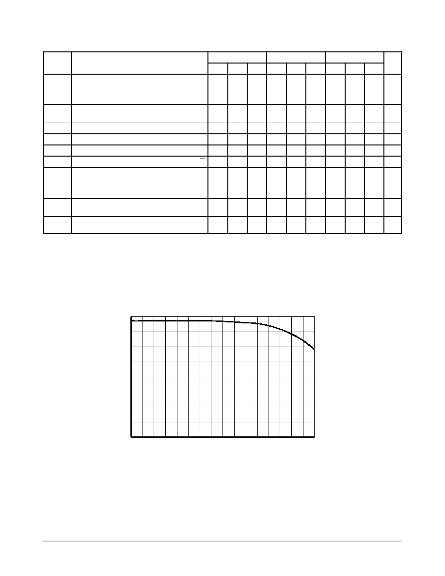
fin, CLOCK INPUT FREQUENCY (GHz)
Figure 3. Output Voltage Amplitude (VOUTPP) vs.
Clock Input Frequency at Ambient Temperature (Typical).
V
OUTP
P,
OUTPUT
VOL
TAGE
AMPLITUDE
(mV)
(TYPICAL)
700
600
500
400
300
200
100
0
4
1
02
800
3
相關(guān)PDF資料 |
PDF描述 |
|---|---|
| NB7V52MMNHTBG | IC FLIP FLOP DATA/CLOCK D 16-QFN |
| NBSG53ABAHTBG | IC CLOCK/DATA DIFF DIV/2 16FCBGA |
| NC7SP74L8X | IC FLIP FLOP ULP D 8-MICROPAK |
| NC7SZ175P6X_F40 | IC FLIP FLOP SGL UHS D SC70-6 |
| NC7SZ373P6 | IC LATCH UHS D 3-STATE SC70-6 |
相關(guān)代理商/技術(shù)參數(shù) |
參數(shù)描述 |
|---|---|
| NB4L6254 | 制造商:ONSEMI 制造商全稱:ON Semiconductor 功能描述:2.5V / 3.3V Differential LVPECL 2x2 Clock Switch and Low Skew Fanout Buffer |
| NB4L6254D | 制造商:ONSEMI 制造商全稱:ON Semiconductor 功能描述:2.5V / 3.3V Differential LVPECL 2x2 Clock Switch and Low Skew Fanout Buffer |
| NB4L6254FAG | 功能描述:模擬和數(shù)字交叉點(diǎn) IC LVPECL 2X2 SW FANOUT RoHS:否 制造商:Micrel 配置:2 x 2 封裝 / 箱體:MLF-16 數(shù)據(jù)速率:10.7 Gbps 輸入電平:CML, LVDS, LVPECL 輸出電平:CML 電源電壓-最大:3.6 V 電源電壓-最小:2.375 V 最大工作溫度:+ 85 C 最小工作溫度:- 40 C 產(chǎn)品:Digital Crosspoint 封裝:Tube |
| NB4L6254FAR2G | 功能描述:模擬和數(shù)字交叉點(diǎn) IC AIT LVPECL 2X2 SW FN RoHS:否 制造商:Micrel 配置:2 x 2 封裝 / 箱體:MLF-16 數(shù)據(jù)速率:10.7 Gbps 輸入電平:CML, LVDS, LVPECL 輸出電平:CML 電源電壓-最大:3.6 V 電源電壓-最小:2.375 V 最大工作溫度:+ 85 C 最小工作溫度:- 40 C 產(chǎn)品:Digital Crosspoint 封裝:Tube |
| NB4L6254MNG | 功能描述:時(shí)鐘驅(qū)動(dòng)器及分配 LVPECL 2X2 SWITCH FANOUT RoHS:否 制造商:Micrel 乘法/除法因子:1:4 輸出類型:Differential 最大輸出頻率:4.2 GHz 電源電壓-最大: 電源電壓-最小:5 V 最大工作溫度:+ 85 C 封裝 / 箱體:SOIC-8 封裝:Reel |
發(fā)布緊急采購,3分鐘左右您將得到回復(fù)。