- 您現在的位置:買賣IC網 > PDF目錄383657 > MXL1001CN8 (MAXIM INTEGRATED PRODUCTS INC) Precision Operational Amplifier PDF資料下載
參數資料
| 型號: | MXL1001CN8 |
| 廠商: | MAXIM INTEGRATED PRODUCTS INC |
| 元件分類: | 運動控制電子 |
| 英文描述: | Precision Operational Amplifier |
| 中文描述: | OP-AMP, 110 uV OFFSET-MAX, 0.8 MHz BAND WIDTH, PDIP8 |
| 封裝: | PLASTIC, DIP-8 |
| 文件頁數: | 2/4頁 |
| 文件大小: | 42K |
| 代理商: | MXL1001CN8 |
M
Prec ision Operational Amplifier
2
_______________________________________________________________________________________
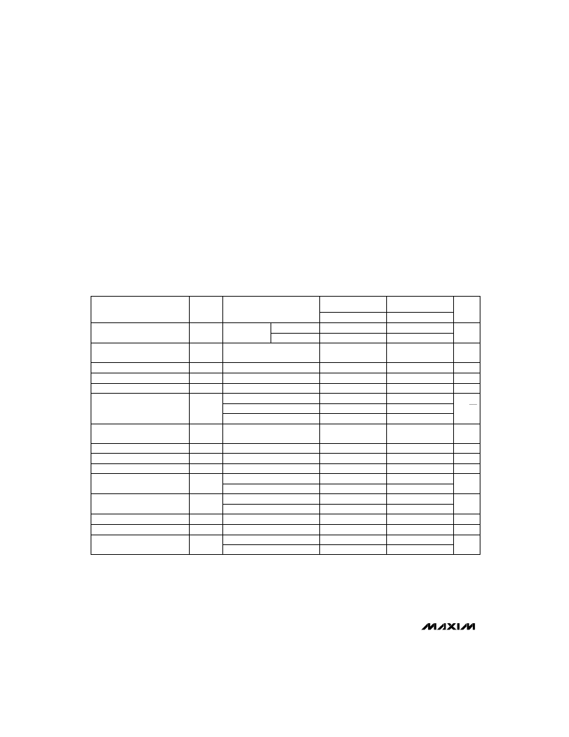
ABSOLUTE MAXIMUM RATINGS
Total Supply Voltage (V+ to V-) ...........................................±22V
Continuous Power Dissipation .........................................500mW
TO-99(H)—derate at 7.1mW/°C above +80°C
CERDIP(J )—derate at 6.7mW/°C above +75°C
Plastic DIP(P)—derate at 5.6mW/°C above +36°C
Small Outline(S)—derate at 5mW/°C above +55°C
Differential Input Voltage .....................................................±30V
Input Voltage (Note 1)..........................................................±22V
ELECTRICAL CHARACTERISTICS
(V
S
= ±15V, T
A
= +25°C, unless otherwise noted.)
Stresses beyond those listed under “Absolute Maximum Ratings” may cause permanent damage to the device. These are stress ratings only, and functional
operation of the device at these or any other conditions beyond those indicated in the operational sections of the specifications is not implied. Exposure to
absolute maximum rating conditions for extended periods may affect device reliability.
Note 2:
MXL1001A grade V
OS
is measured one minute after application of power. For all other grades V
OS
is measured
approximately 0.5 seconds after application of power.
Note 3:
Long-Term Input Offset Voltage Stability refers to the average trend line of V
OS
vs. Time over extended periods after the first
30 days of operation. Excluding the initial hour of operation, changes in V
OS
during the first 30 operating days are typically
2.5μV. Parameter is sample tested.
Note 4:
Sample tested.
Note 5:
Guaranteed by design.
Duration of Output Short Circuit....................................Indefinite
Operating Temperature Ranges:
MXL1001C_/AC_.................................................0°C to +70°C
MXL1001M_/AM_...........................................-55°C to +125°C
J unction Temperature (T
).................................-65°C to +160°C
Storage Temperature Range.............................-65°C to +150°C
Lead Temperature (soldering, 10sec) .............................+300°C
(Note 3)
V
S
= ±3V, no load
V
S
= ±15V, no load
(Note 2)
A
VCL
= +1V (Note 4)
R
L
≥
2k
(Note 4)
R
L
≥
1k
R
L
≥
2k
(Note 5)
R
L
≥
1k
, V
O
= ±10V
R
L
≥
2k
, V
O
= ±12V
f
O
= 1000Hz (Note 4)
f
O
= 100Hz (Note 4)
0.1Hz to 10Hz (Note 4)
f
O
= 10Hz (Note 4)
V
S
= ±3V to ±18V
V
CM
= ±13V
CONDITIONS
mW
4
6
P
D
Power Consumption
46
75
MHz
0.4
0.8
BW
Closed-Loop Bandwidth
V/μs
0.1
0.25
SR
Slew Rate
V
±12.0 ±13.5
V
O
Output Voltage Swing
±13.0 ±14.0
V/mV
300
500
A
VO
Large-Signal Voltage Gain
450
800
dB
110
123
PSRR
Power-Supply Rejection Ratio
dB
114
126
CMRR
Common-Mode Rejection Ratio
μV/
Month
0.2
1.0
V
OS
/Time
Long-Term Input Offset
Voltage Stability
Input Offset Current
Input Bias Current
Input Noise Voltage
μV
10
25
V
OS
7
15
Input Offset Voltage
V
±13
±14
IVR
Input Voltage Range
M
30
100
R
IN
Input Resistance
(Differential Mode)
nV/
√
Hz
9.6
11.0
e
N
Input Noise Voltage Density
10.0
13.0
nA
nA
0.3
±0.5
0.3
10.3
2.0
±2.0
0.6
18.0
I
OS
I
B
e
N p-p
μV
p-p
UNITS
MXL1001AM
MXL1001AC
MIN
TYP
Note 1:
For supply voltages less than ±22V, the absolute maximum input voltage is equal to the supply voltage.
4
8
48
80
0.4
0.8
0.1
0.25
±12.0 ±13.5
±13.0 ±14.0
250
500
400
800
106
123
110
126
0.3
1.5
18
18
60
60
±13
±14
15
80
9.8
11.0
10.0
13.0
0.4
±0.7
0.3
10.5
3.8
±4.0
0.6
18.0
MXL1001M
MXL1001C
MIN
TYP
MAX
SYMBOL
PARAMETER
MAX
MXL1001AC
MXL1001AM
相關PDF資料 |
PDF描述 |
|---|---|
| MXL1001CS8 | Precision Operational Amplifier |
| MXL1001MH | Precision Operational Amplifier |
| MXL1116CS8 | TRANS NPN 55VCEO 50MA SMINI-3 |
| MXL1016CN8 | Ultra-Fast Precision TTL Comparators |
| MXL1116CN8 | Ultra-Fast Precision TTL Comparators |
相關代理商/技術參數 |
參數描述 |
|---|---|
| MXL1001CN8+ | 功能描述:運算放大器 - 運放 RoHS:否 制造商:STMicroelectronics 通道數量:4 共模抑制比(最小值):63 dB 輸入補償電壓:1 mV 輸入偏流(最大值):10 pA 工作電源電壓:2.7 V to 5.5 V 安裝風格:SMD/SMT 封裝 / 箱體:QFN-16 轉換速度:0.89 V/us 關閉:No 輸出電流:55 mA 最大工作溫度:+ 125 C 封裝:Reel |
| MXL1001CS8 | 功能描述:運算放大器 - 運放 RoHS:否 制造商:STMicroelectronics 通道數量:4 共模抑制比(最小值):63 dB 輸入補償電壓:1 mV 輸入偏流(最大值):10 pA 工作電源電壓:2.7 V to 5.5 V 安裝風格:SMD/SMT 封裝 / 箱體:QFN-16 轉換速度:0.89 V/us 關閉:No 輸出電流:55 mA 最大工作溫度:+ 125 C 封裝:Reel |
| MXL1001CS8+ | 功能描述:運算放大器 - 運放 RoHS:否 制造商:STMicroelectronics 通道數量:4 共模抑制比(最小值):63 dB 輸入補償電壓:1 mV 輸入偏流(最大值):10 pA 工作電源電壓:2.7 V to 5.5 V 安裝風格:SMD/SMT 封裝 / 箱體:QFN-16 轉換速度:0.89 V/us 關閉:No 輸出電流:55 mA 最大工作溫度:+ 125 C 封裝:Reel |
| MXL1001CS8+T | 功能描述:運算放大器 - 運放 RoHS:否 制造商:STMicroelectronics 通道數量:4 共模抑制比(最小值):63 dB 輸入補償電壓:1 mV 輸入偏流(最大值):10 pA 工作電源電壓:2.7 V to 5.5 V 安裝風格:SMD/SMT 封裝 / 箱體:QFN-16 轉換速度:0.89 V/us 關閉:No 輸出電流:55 mA 最大工作溫度:+ 125 C 封裝:Reel |
| MXL1001CS8-T | 功能描述:運算放大器 - 運放 RoHS:否 制造商:STMicroelectronics 通道數量:4 共模抑制比(最小值):63 dB 輸入補償電壓:1 mV 輸入偏流(最大值):10 pA 工作電源電壓:2.7 V to 5.5 V 安裝風格:SMD/SMT 封裝 / 箱體:QFN-16 轉換速度:0.89 V/us 關閉:No 輸出電流:55 mA 最大工作溫度:+ 125 C 封裝:Reel |
發(fā)布緊急采購,3分鐘左右您將得到回復。