- 您現(xiàn)在的位置:買賣IC網(wǎng) > PDF目錄383644 > MT9040 (Mitel Networks Corporation) T1/E1 Synchronizer(T1/E1 系統(tǒng)同步裝置(由一個數(shù)字鎖相環(huán)組成)) PDF資料下載
參數(shù)資料
| 型號: | MT9040 |
| 廠商: | Mitel Networks Corporation |
| 英文描述: | T1/E1 Synchronizer(T1/E1 系統(tǒng)同步裝置(由一個數(shù)字鎖相環(huán)組成)) |
| 中文描述: | 的T1/E1同步(T1/E1的系統(tǒng)同步裝置(由一個數(shù)字鎖相環(huán)組成)) |
| 文件頁數(shù): | 2/20頁 |
| 文件大小: | 82K |
| 代理商: | MT9040 |
MT9040
Advance Information
2
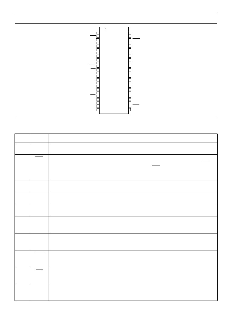
Figure 2 - Pin Connections
Pin Description
Pin #
Name
Description
1,10,
23,31
V
SS
Ground.
0 Volts. (Vss pads).
2
RST
Reset (Input).
A logic low at this input resets the MT9040. To ensure proper operation, the
device must be reset after reference signal frequency changes and power-up. The RST pin
should be held low for a minimum of 300ns. While the RST pin is low, all frame and clock
outputs are at logic high. Following a reset, the input reference source and output clocks and
frame pulses are phase aligned as shown in Figure 9.
3,4,5,
38,43
IC
Internal Connection.
Leave open circuit.
6
REF
Reference (Input).
This is the input reference source (falling edge) used for synchronization.
One of four possible frequencies (8kHz, 1.544MHz, 2.048MHz or 19.44MHz) may be used.
7,17
28,35
V
DD
Positive Supply Voltage.
+3.3V
DC
nominal.
8
OSCo
Oscillator Master Clock (CMOS Output).
For crystal operation, a 20MHz crystal is
connected from this pin to OSCi, see Figure 6. For clock oscillator operation, this pin is left
unconnected, see Figure 5.
9
OSCi
Oscillator Master Clock (CMOS Input).
For crystal operation, a 20MHz crystal is connected
from this pin to OSCo, see Figure 6. For clock oscillator operation, this pin is connected to a
clock source, see Figure 5.
11
F16o
Frame Pulse ST-BUS 8.192 Mb/s (CMOS Output).
This is an 8kHz 61ns active low framing
pulse, which marks the beginning of an ST-BUS frame. This is typically used for ST-BUS
operation at 8.192 Mb/s. See Figure 10.
12
F0o
Frame Pulse ST-BUS 2.048Mb/s (CMOS Output).
This is an 8kHz 244ns active low framing
pulse, which marks the beginning of an ST-BUS frame. This is typically used for ST-BUS
operation at 2.048Mb/s and 4.096Mb/s. See Figure 10.
13
RSP
Receive Sync Pulse (CMOS Output).
This is an 8kHz 488ns active high framing pulse, which
marks the beginning of an ST-BUS frame. This is typically used for connection to the Siemens
MUNICH-32 device. See Figure 11.
2
3
4
5
6
7
8
9
10
11
12
13
14
15
16
17
18
19
20
21
22
23
24
1
47
46
45
44
43
42
41
40
39
38
37
36
35
34
33
32
31
30
29
28
27
26
25
TRST
TDI
TDO
IC
IC
FS1
FS2
IC
IC
IC
MS
Vdd
IC
IC
NC
Vss
IC
IM
Vdd
C6o
C16o
RST
IC
IC
REF
Vdd
OSCo
OSCi
Vss
F16o
F0o
TSP
F8o
C1.5o
Vdd
LOCK
C2o
C4o
C19o
FLOCK
48
TMS
TCK
V
SS
Vss
IC
C8o
MT9040AN
RSP
IC
相關PDF資料 |
PDF描述 |
|---|---|
| MT9041A | () |
| MT9041B | T1/E1 System Synchronizer(T1/E1系統(tǒng)同步裝置(由一個數(shù)字鎖相環(huán)組成)) |
| MT9042B | () |
| MT9042C | Multitrunk System Synchronizer(多中繼系統(tǒng)同步裝置) |
| MT9043 | T1/E1 System Synchronizer(T1/E1 系統(tǒng)同步裝置(由一個數(shù)字鎖相環(huán)組成)) |
相關代理商/技術參數(shù) |
參數(shù)描述 |
|---|---|
| MT90401 | 制造商:ZARLINK 制造商全稱:Zarlink Semiconductor Inc 功能描述:SONET/SDH Clock Multiplier PLL |
| MT90401AB | 制造商:ZARLINK 制造商全稱:Zarlink Semiconductor Inc 功能描述:SONET/SDH System Synchronizer |
| MT90401AB1 | 制造商:Microsemi Corporation 功能描述:FRAMER SDH/SONET 3.3V 80LQFP EP - Trays 制造商:MICROSEMI CONSUMER MEDICAL PRODUCT GROUP 功能描述:IC SYNCHRONIZER SONET/SDH 80LQFP 制造商:Microsemi Corporation 功能描述:IC SYNCHRONIZER SONET/SDH 80LQFP |
| MT9040AN | 制造商:ZARLINK 制造商全稱:Zarlink Semiconductor Inc 功能描述:T1/E1 Synchronizer |
| MT9040AN1 | 制造商:Microsemi Corporation 功能描述:FRAMER E1 /T1 3.3V 48SSOP - Rail/Tube |
發(fā)布緊急采購,3分鐘左右您將得到回復。