- 您現(xiàn)在的位置:買賣IC網(wǎng) > PDF目錄384759 > MT8LDT864HX (Micron Technology, Inc.) SMALL-OUTLINE DRAM MODULE PDF資料下載
參數(shù)資料
| 型號(hào): | MT8LDT864HX |
| 廠商: | Micron Technology, Inc. |
| 英文描述: | SMALL-OUTLINE DRAM MODULE |
| 中文描述: | 小外形DRAM模塊 |
| 文件頁(yè)數(shù): | 5/32頁(yè) |
| 文件大小: | 625K |
| 代理商: | MT8LDT864HX |
第1頁(yè)第2頁(yè)第3頁(yè)第4頁(yè)當(dāng)前第5頁(yè)第6頁(yè)第7頁(yè)第8頁(yè)第9頁(yè)第10頁(yè)第11頁(yè)第12頁(yè)第13頁(yè)第14頁(yè)第15頁(yè)第16頁(yè)第17頁(yè)第18頁(yè)第19頁(yè)第20頁(yè)第21頁(yè)第22頁(yè)第23頁(yè)第24頁(yè)第25頁(yè)第26頁(yè)第27頁(yè)第28頁(yè)第29頁(yè)第30頁(yè)第31頁(yè)第32頁(yè)
4, 8 Meg x 64 DRAM SODIMMs
DM83.p65 – Rev. 2/99
Micron Technology, Inc., reserves the right to change products or specifications without notice.
1999, Micron Technology, Inc.
5
4, 8 MEG x 64
DRAM SODIMMs
STANDBY
Returning RAS# and CAS# HIGH terminates a
memory cycle and decreases chip current to a reduced
standby level. Also, the chip is preconditioned for the
next cycle during the RAS# HIGH time.
SERIAL PRESENCE-DETECT OPERATION
This module family incorporates serial presence-
detect (SPD). The SPD function is implemented using
a 2,048-bit EEPROM. This nonvolatile storage device
contains 256 bytes. The first 128 bytes can be pro-
grammed by Micron to identify the module type and
various DRAM organizations and timing parameters.
The remaining 128 bytes of storage are available for use
by the customer. System READ/WRITE operations be-
tween the master (system logic) and the slave EEPROM
device (DIMM) occur via a standard IIC bus using the
DIMM’s SCL (clock) and SDA (data) signals.
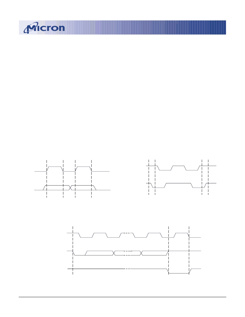
SPD CLOCK AND DATA CONVENTIONS
Data states on the SDA line can change only during
SCL LOW. SDA state changes during SCL HIGH are
reserved for indicating start and stop conditions (Fig-
ures 1 and 2).
SPD START CONDITION
All commands are preceded by the start condition,
which is a HIGH-to-LOW transition of SDA when SCL
is HIGH. The SPD device continuously monitors the
SDA and SCL lines for the start condition and will not
respond to any command until this condition has
been met.
SPD STOP CONDITION
All communications are terminated by a stop con-
dition, which is a LOW-to-HIGH transition of SDA
when SCL is HIGH. The stop condition is also used to
place the SPD device into standby power mode.
SPD A CKNOWLEDGE
Acknowledge is a software convention used to
indicate successful data transfers. The transmitting
device, either master or slave, will release the bus after
transmitting eight bits. During the ninth clock cycle,
the receiver will pull the SDA line LOW to acknowledge
that it received the eight bits of data (Figure 3).
The SPD device will always respond with an ac-
knowledge after recognition of a start condition and
its slave address. If both the device and a WRITE
Figure 3
Acknow ledge Response From Receiver
SCL from Master
Data Output
from Transmitter
Data Output
from Receiver
9
8
Acknowledge
Figure 2
Definition of Start and Stop
SCL
SDA
START
BIT
STOP
BIT
Figure 1
Data Validity
SCL
SDA
DATA STABLE
DATA STABLE
DATA
CHANGE
相關(guān)PDF資料 |
PDF描述 |
|---|---|
| MT4LDT464H | SMALL-OUTLINE DRAM MODULE |
| MT4LDT464HS | SMALL-OUTLINE DRAM MODULE |
| MT4LDT464HX | SMALL-OUTLINE DRAM MODULE |
| MT8LSDT864 | SMALL-OUTLINE SDRAM MODULE |
| MT4LSDT464H | SMALL-OUTLINE SDRAM MODULE |
相關(guān)代理商/技術(shù)參數(shù) |
參數(shù)描述 |
|---|---|
| MT8LDT864HXS | 制造商:MICRON 制造商全稱:Micron Technology 功能描述:SMALL-OUTLINE DRAM MODULE |
| MT8LLN21PADF-A | 制造商:Micron Technology Inc 功能描述:COPPERHEAD CHIPSET - Trays |
| MT8LLN21PADFA2 | 制造商:Micron Technology Inc 功能描述:COPPERHEAD CHIP 制造商:Micron Technology 功能描述:COPPERHEAD CHIP |
| MT8LLN21PADF-A2 | 制造商:Micron Technology Inc 功能描述:COPPERHEAD CHIP 制造商:Micron Technology 功能描述:COPPERHEAD CHIP |
| MT8LLN22NCNE-A | 制造商:Micron Technology Inc 功能描述:COPPERTAIL CHIPSET - Trays |
發(fā)布緊急采購(gòu),3分鐘左右您將得到回復(fù)。