- 您現(xiàn)在的位置:買賣IC網(wǎng) > PDF目錄359234 > MT8986APR1 (Toshiba Corporation) CMOS ST-BUS Family Multiple Rate Digital Switch PDF資料下載
參數(shù)資料
| 型號: | MT8986APR1 |
| 廠商: | Toshiba Corporation |
| 英文描述: | CMOS ST-BUS Family Multiple Rate Digital Switch |
| 中文描述: | 意法半導(dǎo)體的CMOS總線家庭多速率數(shù)字開關(guān) |
| 文件頁數(shù): | 3/46頁 |
| 文件大小: | 765K |
| 代理商: | MT8986APR1 |
第1頁第2頁當(dāng)前第3頁第4頁第5頁第6頁第7頁第8頁第9頁第10頁第11頁第12頁第13頁第14頁第15頁第16頁第17頁第18頁第19頁第20頁第21頁第22頁第23頁第24頁第25頁第26頁第27頁第28頁第29頁第30頁第31頁第32頁第33頁第34頁第35頁第36頁第37頁第38頁第39頁第40頁第41頁第42頁第43頁第44頁第45頁第46頁
MT8986
Data Sheet
3
Zarlink Semiconductor Inc.
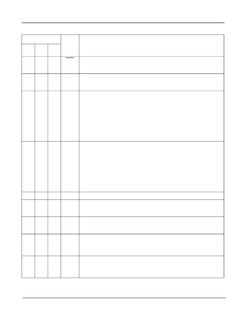
Pin Description
Pin #
Name
Description
40
DIP
44
PLCC
44
QFP
1
2
40
DTA
Data Acknowledgement
(Open Drain Output)
.
This active low output indicates
that a data bus transfer is complete. A 10 k
pull-up resistor is required at this
output.
2-7
3-5
7-9
41-43
1-3
STi0-5
ST-BUS Inputs 0 to 5
(Inputs). Serial data input streams. These streams may
have data rates of 2.048, 4.096 or 8.192 Mbit/s with 32, 64 or 128 channels,
respectively.
8
10
4
STi6/A6
ST-BUS Input 6/Addr.6 input
(Input). The function of this pin is determined by
the switching configuration enabled. If non-multiplexed CPU bus is used along
with a higher input rate of 8.192 or 4.096 Mb/s, this pin provides A6 address
input function. For 2.048 and 4.096 Mb/s (8x4) applications or when multiplexed
CPU bus (44 pin only) is selected, this pin assumes STi6 function. See Control
Register bits description and Tables 1, 2, 6 & 7 for more details.
Note that for applications where both A6 and STi6 inputs are required
simultaneously (e.g., 8 x 4 switching configuration at 4.096 Mb/s or rate
conversion between 2.048 Mb/s to 4.196 or 8.192 Mb/s) the A6 input should be
connected to pin STo6/A6.
9
11
5
STi7/A7
ST-BUS Input 7/Addr.7 input
(Input): The function of this pin is determined by
the switching configuration enabled. If non-multiplexed CPU bus is used along
with a higher input rate of 8.192 Mb/s, this pin provides A7 address input
function.
For 2.048 and 4.096 Mb/s (8x4) applications or when multiplexed CPU bus
(44 pin only) is selected, this pin assumes STi7 function. See Control Register
bits description and Tables 1, 2, 6 & 7 for more details.
Note that for applications where both A7 and STi7 inputs are required
simultaneously (e.g., 2.048 to 8.192 Mb/s rate conversion) the A7 input should
be connected to pin STo7/A7.
10
12
6
V
DD
+5 Volt Power Supply.
11
13
7
FR
Frame Pulse
(Input). This input accepts and automatically identifies frame
synchronization signals formatted according to ST-BUS and GCI interface
specifications.
12
14
8
CLK
Clock
(Input). Serial clock for shifting data in/out on the serial streams.
Depending on the serial interface speed selected by IMS (Interface Mode Select)
register, the clock at this pin can be 4.096 or 8.192 MHz.
13-15
15-17
9-11
A0-2/
STi8-10
Address 0-2 / Input Streams 8-10
(Input). When non-multiplexed CPU bus is
selected, these lines provide the A0-A2 address lines to MT8986 internal
registers. When 16x8 switching configuration is selected (in 44 pin only), then
these pins are ST-BUS serial inputs 8 to 10 receiving data at 2.048 Mb/s.
16-18
19-21
13-15
A3-5/
STi11-13
Address 3-5 / Input Streams 11-13
(Input). When non-multiplexed CPU bus is
selected, these lines provide the A3-A5 address lines to MT8986 internal
registers. When 16x8 switching configuration is selected (in 44 pin only), then
these pins are ST-BUS serial inputs 11 to 13 receiving data at 2.048 Mb/s.
相關(guān)PDF資料 |
PDF描述 |
|---|---|
| MT8986APR | CMOS ST-BUS Family Multiple Rate Digital Switch |
| MT8986AP1 | CMOS ST-BUS Family Multiple Rate Digital Switch |
| MT8986AP | CMOS ST-BUS Family Multiple Rate Digital Switch |
| MT8986AL | CMOS ST-BUS Family Multiple Rate Digital Switch |
| MT8986 | CMOS ST-BUS⑩ FAMILY Multiple Rate Digital Switch |
相關(guān)代理商/技術(shù)參數(shù) |
參數(shù)描述 |
|---|---|
| MT8992BC | 制造商:MITEL 制造商全稱:Mitel Networks Corporation 功能描述:Digital Telephone with HDLC |
| MT8993BC | 制造商:MITEL 制造商全稱:Mitel Networks Corporation 功能描述:Digital Telephone with HDLC |
| MT89L80 | 制造商:MITEL 制造商全稱:Mitel Networks Corporation 功能描述:CMOS ST-BUS⑩ FAMILY Digital Switch |
| MT89L80AN | 制造商:Microsemi Corporation 功能描述: |
| MT89L80AN1 | 制造商:Microsemi Corporation 功能描述:SWIT FABRIC 256 X 256 16.384MBPS 3.3V 48SSOP /BAKE/DRYPACK - Rail/Tube |
發(fā)布緊急采購,3分鐘左右您將得到回復(fù)。