- 您現(xiàn)在的位置:買賣IC網(wǎng) > PDF目錄384758 > MT88L89 (Mitel Networks Corporation) 3V Integrated DTMF Transceiver with Adaptive Micro Interface(3V 集成雙音多頻信號(DTMF)接收器(帶自適應(yīng)微接口)) PDF資料下載
參數(shù)資料
| 型號: | MT88L89 |
| 廠商: | Mitel Networks Corporation |
| 英文描述: | 3V Integrated DTMF Transceiver with Adaptive Micro Interface(3V 集成雙音多頻信號(DTMF)接收器(帶自適應(yīng)微接口)) |
| 中文描述: | 3V的雙音多頻收發(fā)器集成自適應(yīng)微型接口(3V的集成雙音多頻信號(DTMF)的接收器(帶自適應(yīng)微接口)) |
| 文件頁數(shù): | 9/28頁 |
| 文件大小: | 210K |
| 代理商: | MT88L89 |
第1頁第2頁第3頁第4頁第5頁第6頁第7頁第8頁當(dāng)前第9頁第10頁第11頁第12頁第13頁第14頁第15頁第16頁第17頁第18頁第19頁第20頁第21頁第22頁第23頁第24頁第25頁第26頁第27頁第28頁
MT88L89
4-131
Continuous activity on DS/RD is not necessary
to update the internal status registers.
Compatible with Motorola and Intel processors.
Determines whether input timing is that of an
Intel or Motorola controller by monitoring
DS/RD, on the CS falling edge.
Differentiates between multiplexed and non-
multiplexed microprocessor buses. Address and
data are latched in accordingly.
Figure 17 shows the timing diagram for the Motorola
microcontrollers. The chip select (CS) input is formed
by NANDing address strobe (AS) and address
decode output. The MT88L89 examines the state of
DS/RD on the falling edge of CS. For Motorola bus
timing DS/RD must be low on the falling edge of CS.
Figure 12(a) shows the connection of the MC68L11/
MC68B11 Motorola processor to the MT88L89
DTMF transceiver.
Figures 18 and 19 are the timing diagrams for the
Intel 8xL5x series (12 MHz) micro-controllers with
multiplexed address and data buses. The MT88L89
latches in the state of DS/RD on the falling edge of
CS. When DS/RD is high, Intel processor operation
is selected. By NANDing the address latch enable
(ALE) output with the high-byte address (P2) decode
output, CS can be generated. Figure 12(b) shows
the connection of these Intel processors to the
MT88L89 transceiver.
NOTE:
The adaptive micro interface relies on high-
to-low
transition
on
microcontroller interface. This pin must not be tied
permanently low. Only one register access is allowed
on any CS assertion.
CS
to
recognize
the
The adaptive micro interface provides access to five
internal registers. The read-only Receive Data
Register contains the decoded output of the last valid
DTMF digit received. Data entered into the write-only
Transmit Data Register will determine which tone
pair is to be generated (see Table 1 for coding
details). Transceiver control is accomplished with two
control registers (see Tables 6 and 7), CRA and
CRB, which have the same address. A write
operation to CRB is executed by first setting the most
significant bit (b3) in CRA. The following write
operation to the same address will then be directed
to CRB, and subsequent write cycles will be directed
back to CRA. The read-only status register indicates
the current transceiver state (see Table 8).
A software reset must be included at the beginning
of all programs to initialize the control registers upon
power-up or power reset (see Figure 15). Refer to
Tables 4-7 for bit descriptions of the two control
registers.
The multiplexed IRQ/CP pin can be programmed to
generate an interrupt upon validation of DTMF
signals or when the transmitter is ready for more
data (burst mode only). Alternatively, this pin can be
configured to provide a square-wave output of the
call progress signal. The IRQ/CP pin is an open drain
output and requires an external pull-up resistor (see
Figure 13 and Figure 14).
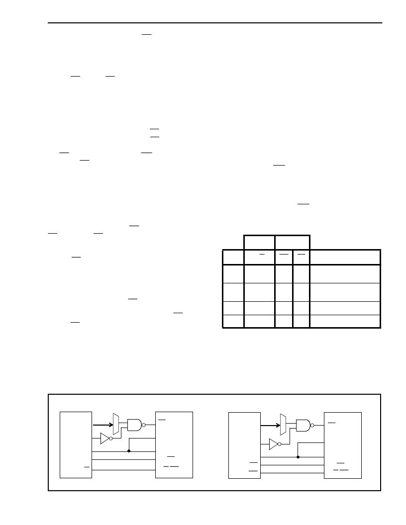
Table 3. Internal Register Functions
Motorola
Intel
RS0
R/W
WR
RD
FUNCTION
0
0
0
1
Write to Transmit
Data Register
0
1
1
0
Read from Receive
Data Register
1
0
0
1
Write to Control Register
1
1
1
0
Read from Status Register
Figure 12 a) & b) - MT88L89 Interface Connections for Various Intel and Motorola Micros
MT88L89
MC68L11/
MC68B11
MT88L89
8xL5x
A8-A15
AS
AD0-AD3
RW
CS
RS0
DS/RD
D0-D3
R/W/WR
E
A8-A15
ALE
P0
RD
WR
CS
D0-D3
RS0
DS/RD
R/W/WR
12 (b) Intel
12 (a) Motorola
相關(guān)PDF資料 |
PDF描述 |
|---|---|
| MT88V32 | 8 x 4 High Performance Video Switch Array(8 x 4 高性能數(shù)字可編程正交開關(guān)(用于控制寬帶視頻信號)) |
| MT8910-1 | CMOS ST-BUS⑩ FAMILY Digital Subscriber Line Interface Circuit |
| MT8910-1AC | CMOS ST-BUS⑩ FAMILY Digital Subscriber Line Interface Circuit |
| MT8910-1AP | CMOS ST-BUS⑩ FAMILY Digital Subscriber Line Interface Circuit |
| MT8920 | ISO-CMOS ST-BUS⑩ FAMILY ST-BUS Parallel Access Circuit |
相關(guān)代理商/技術(shù)參數(shù) |
參數(shù)描述 |
|---|---|
| MT88L89AC | 制造商:MITEL 制造商全稱:Mitel Networks Corporation 功能描述:3V Integrated DTMFTransceiver with Adaptive Micro Interface |
| MT88L89AE | 制造商:MITEL 制造商全稱:Mitel Networks Corporation 功能描述:3V Integrated DTMFTransceiver with Adaptive Micro Interface |
| MT88L89AN | 制造商:Microsemi Corporation 功能描述: |
| MT88L89AN1 | 制造商:Microsemi Corporation 功能描述:DTMF TXRX 3.58MHZ CMOS 3V 24SSOP - Rail/Tube |
| MT88L89ANR1 | 制造商:Microsemi Corporation 功能描述:DTMF TXRX 3.58MHZ CMOS 3V 24SSOP - Tape and Reel 制造商:MICROSEMI CONSUMER MEDICAL PRODUCT GROUP 功能描述:IC TXRX DTMF 3V 24SSOP 制造商:Microsemi Corporation 功能描述:IC TXRX DTMF 3V 24SSOP |
發(fā)布緊急采購,3分鐘左右您將得到回復(fù)。