- 您現(xiàn)在的位置:買賣IC網(wǎng) > PDF目錄383642 > MT88L85AP (Mitel Networks Corporation) 3V Integrated DTMFTransceiver with Power Down & Adaptive Micro Interface PDF資料下載
參數(shù)資料
| 型號: | MT88L85AP |
| 廠商: | Mitel Networks Corporation |
| 英文描述: | 3V Integrated DTMFTransceiver with Power Down & Adaptive Micro Interface |
| 中文描述: | 3V的集成DTMFTransceiver與掉電 |
| 文件頁數(shù): | 8/20頁 |
| 文件大小: | 350K |
| 代理商: | MT88L85AP |
MT88L85
Advance Information
4-78
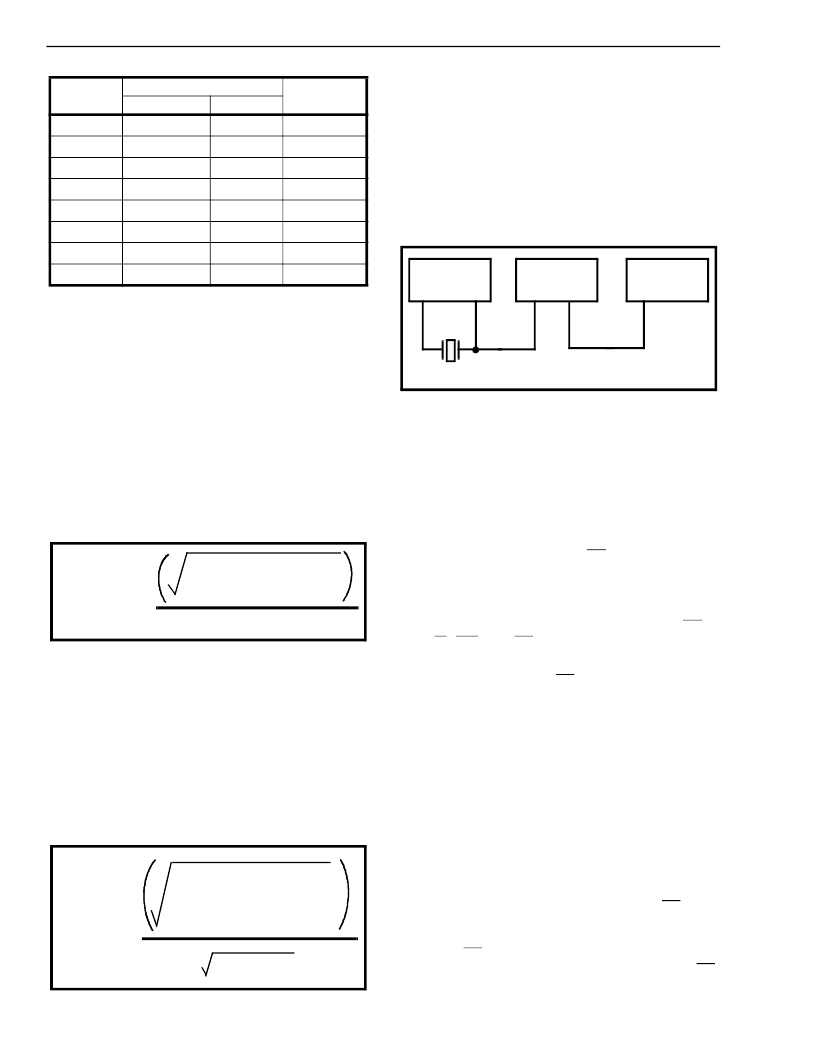
Table 2. Actual Frequencies Versus Standard
Requirements
Distortion Calculations
The MT88L85 is capable of producing precise tone
bursts with minimal error in frequency (see Table 2).
The internal summing amplifier is followed by a first-
order lowpass switched capacitor filter to minimize
harmonic components and intermodulation products.
The total harmonic distortion for a single tone can be
calculated using Equation 1, which is the ratio of the
total power of all the extraneous frequencies to the
power of the fundamental frequency expressed as a
percentage.
Equation 1. THD (%) For a Single Tone
The Fourier components of the tone output
correspond to V
2f
.... V
nf
as measured on the output
waveform. The total harmonic distortion for a dual
tone can be calculated using Equation 2. V
L
and V
H
correspond to the low group amplitude and high
group amplitude, respectively and V
2IMD
is the sum
of all the intermodulation components. The internal
switched-capacitor filter following the D/A converter
keeps distortion products down to a very low level as
shown in Figure 10.
Equation 2. THD (%) For a Dual Tone
ACTIVE
INPUT
OUTPUT FREQUENCY (Hz)
%ERROR
SPECIFIED
697
770
852
941
1209
1336
1477
1633
ACTUAL
699.1
766.2
847.4
948.0
1215.9
1331.7
1471.9
1645.0
L1
+0.30
-0.49
-0.54
+0.74
+0.57
-0.32
-0.35
+0.73
L2
L3
L4
H1
H2
H3
H4
THD (%) = 100
V
fundamental
V
2
2f
+ V
2
3f
+ V
2
4f
+ .... V
2
nf
V
2L
+
V
2H
V
22L
+
V
23L
+ ....
V
2nL
+
V
22H
+
V
23H
+ ..
V
2nH
+
V
2IMD
THD (%) = 100
DTMF Clock Circuit
The internal clock circuit is completed with the
addition of a standard television colour burst crystal
having a resonant frequency of 3.579545 MHz. A
number of MT88L85 devices can be connected as
shown in Figure 11 such that only one crystal is
required. Alternatively, the OSC1 inputs on all
devices can be driven from a TTL buffer with the
OSC2 outputs left unconnected.
Figure 11 - Common Crystal Connection
Microprocessor Interface
The MT88L85 design incorporates an adaptive
interface, which allows it to be connected to various
kinds of microprocessors. Key functions of this
interface include the following:
Continuous activity on DS/RD is not necessary
to update the internal status registers.
senses whether input timing is that of an Intel or
Motorola controller by monitoring the
DS (RD),
R/W (WR) and CS inputs.
generates equivalent CS signal for internal
operation for all processors.
differentiates between multiplexed and non-
multiplexed microprocessor buses. Address
and data are latched in accordingly.
compatible with Motorola and Intel processors.
Figure 16 shows the timing diagram for Motorola
microprocessors with separate address and data
buses. Members of this microprocessor family
include 2 MHz versions of the MC6800, MC6802 and
MC6809. For the MC6809, the chip select (CS) input
signal is formed by NANDing the (E+Q) clocks and
address decode output. For the MC6800 and
MC6802, CS is formed by NANDing VMA and
address decode output. On the falling edge of CS,
the internal logic senses the state of data strobe
MT88L85
OSC1
OSC2
MT88L85
OSC1
OSC2
MT88L85
OSC1
OSC2
3.579545 MHz
相關(guān)PDF資料 |
PDF描述 |
|---|---|
| MT88L89 | 3V Integrated DTMFTransceiver with Adaptive Micro Interface |
| MT88L89AC | 3V Integrated DTMFTransceiver with Adaptive Micro Interface |
| MT88L89AE | 3V Integrated DTMFTransceiver with Adaptive Micro Interface |
| MT88L89AN | 3V Integrated DTMFTransceiver with Adaptive Micro Interface |
| MT88L89AP | 3V Integrated DTMFTransceiver with Adaptive Micro Interface |
相關(guān)代理商/技術(shù)參數(shù) |
參數(shù)描述 |
|---|---|
| MT88L89 | 制造商:MITEL 制造商全稱:Mitel Networks Corporation 功能描述:3V Integrated DTMFTransceiver with Adaptive Micro Interface |
| MT88L89AC | 制造商:MITEL 制造商全稱:Mitel Networks Corporation 功能描述:3V Integrated DTMFTransceiver with Adaptive Micro Interface |
| MT88L89AE | 制造商:MITEL 制造商全稱:Mitel Networks Corporation 功能描述:3V Integrated DTMFTransceiver with Adaptive Micro Interface |
| MT88L89AN | 制造商:Microsemi Corporation 功能描述: |
| MT88L89AN1 | 制造商:Microsemi Corporation 功能描述:DTMF TXRX 3.58MHZ CMOS 3V 24SSOP - Rail/Tube |
發(fā)布緊急采購,3分鐘左右您將得到回復(fù)。