- 您現(xiàn)在的位置:買賣IC網(wǎng) > PDF目錄384758 > MT8889CC-1 (Mitel Networks Corporation) Integrated DTMFTransceiver with Adaptive Micro Interface PDF資料下載
參數(shù)資料
| 型號: | MT8889CC-1 |
| 廠商: | Mitel Networks Corporation |
| 英文描述: | Integrated DTMFTransceiver with Adaptive Micro Interface |
| 中文描述: | 綜合DTMFTransceiver自適應(yīng)微型接口 |
| 文件頁數(shù): | 2/18頁 |
| 文件大?。?/td> | 356K |
| 代理商: | MT8889CC-1 |
MT8889C/MT8889C-1
4-108
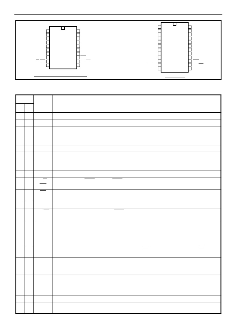
Figure 2 - Pin Connections
Pin Description
Pin #
Name
Description
20
24
1
1
IN+
Non-inverting
op-amp input.
2
2
IN-
Inverting
op-amp input.
3
3
GS
Gain Select
. Gives access to output of front end differential amplifier for connection of
feedback resistor.
4
4
V
Ref
V
SS
OSC1
Reference Voltage
output (V
DD
/2).
Ground (0V).
5
5
6
6
Oscillator
input. This pin can also be driven directly by an external clock.
7
7
OSC2
Oscillator
output. A 3.579545 MHz crystal connected between OSC1 and OSC2 completes
the internal oscillator circuit. Leave open circuit when OSC1 is driven externally.
8
10
TONE
Output from internal DTMF transmitter.
9
11
R/W
(
WR
)
(Motorola)
Read/Write
or (Intel)
Write
microprocessor input. TTL compatible.
10
12
CS
Chip Select
input. This signal must be qualified externally by either address strobe (AS),
valid memory address (VMA) or address latch enable (ALE) signal, see Figure 12.
11
13
RS0
Register Select
input. Refer to Table 3 for bit interpretation. TTL compatible.
12
14
DS
(
RD) (Motorola)
Data Strobe
or (Intel)
Read
microprocessor input. Activity on this input is only
required when the device is being accessed. TTL compatible.
13
15
IRQ/CP
Interrupt Request/Call Progress
(open drain) output. In interrupt mode, this output goes
low when a valid DTMF tone burst has been transmitted or received. In call progress mode,
this pin will output a rectangular signal representative of the input signal applied at the input
op-amp. The input signal must be within the bandwidth limits of the call progress filter, see
Figure 8.
14-
17
18-
21
D0-D3
Microprocessor data bus. High impedance when CS = 1 or DS =0 (Motorola) or RD = 1
(Intel). TTL compatible.
18
22
ESt
Early Steering
output. Presents a logic high once the digital algorithm has detected a valid
tone pair (signal condition). Any momentary loss of signal condition will cause ESt to return
to a logic low.
19
23
St/GT
Steering Input/Guard Time
output (bidirectional). A voltage greater than V
TSt
detected at
St causes the device to register the detected tone pair and update the output latch. A
voltage less than V
TSt
frees the device to accept a new tone pair. The GT output acts to
reset the external steering time-constant; its state is a function of ESt and the voltage on St.
20
24
V
DD
NC
Positive power supply (5V typ.).
8,9
16,
17
No Connection.
1
2
3
4
5
6
7
8
9
10
11
12
20
19
18
17
16
15
14
13
IN+
IN-
GS
VRef
VSS
OSC1
OSC2
TONE
R/W/WR
CS
VDD
St/GT
ESt
D3
D2
D1
D0
IRQ/CP
DS/RD
RS0
NC
NC
1
2
3
4
5
6
7
8
9
10
11
12
13
14
15
16
24
23
22
21
20
19
18
17
IN+
IN-
GS
VRef
VSS
OSC1
OSC2
TONE
R/W/WR
CS
VDD
St/GT
ESt
D3
D2
D1
D0
NC
NC
IRQ/CP
DS/RD
RS0
24 PIN SSOP
20 PIN CERDIP/PLASTIC DIP/SOIC
相關(guān)PDF資料 |
PDF描述 |
|---|---|
| MT8889CN-1 | Integrated DTMFTransceiver with Adaptive Micro Interface |
| MT8889CS-1 | Integrated DTMFTransceiver with Adaptive Micro Interface |
| MT8889C | Integrated DTMFTransceiver with Adaptive Micro Interface |
| MT8889CC | Integrated DTMFTransceiver with Adaptive Micro Interface |
| MT8889CE | Integrated DTMFTransceiver with Adaptive Micro Interface |
相關(guān)代理商/技術(shù)參數(shù) |
參數(shù)描述 |
|---|---|
| MT8889CE | 制造商:Microsemi Corporation 功能描述: |
| MT8889CE1 | 制造商:Microsemi Corporation 功能描述: 制造商:Microsemi Corporation 功能描述:DTMF TXRX 3.58MHZ CMOS 5V 20PDIP - Rail/Tube 制造商:MICROSEMI CONSUMER MEDICAL PRODUCT GROUP 功能描述:IC TXRX DTMF 20PDIP 制造商:Microsemi Corporation 功能描述:IC TXRX DTMF 20PDIP |
| MT8889CE-1 | 制造商:MITEL 制造商全稱:Mitel Networks Corporation 功能描述:Integrated DTMFTransceiver with Adaptive Micro Interface |
| MT8889CN | 制造商:Microsemi Corporation 功能描述: |
| MT8889CN1 | 制造商:Microsemi Corporation 功能描述:DTMF TXRX 3.58MHZ CMOS 5V 24SSOP - Rail/Tube 制造商:MICROSEMI CONSUMER MEDICAL PRODUCT GROUP 功能描述:IC TXRX DTMF 24SSOP 制造商:Microsemi Corporation 功能描述:IC TXRX DTMF 24SSOP |
發(fā)布緊急采購,3分鐘左右您將得到回復(fù)。