- 您現(xiàn)在的位置:買賣IC網(wǎng) > PDF目錄383640 > MT8809 (Mitel Networks Corporation) ISO-CMOS 8 x 8 Analog Switch Array PDF資料下載
參數(shù)資料
| 型號: | MT8809 |
| 廠商: | Mitel Networks Corporation |
| 英文描述: | ISO-CMOS 8 x 8 Analog Switch Array |
| 中文描述: | 標準- 8 × 8的CMOS模擬開關陣列 |
| 文件頁數(shù): | 5/6頁 |
| 文件大小: | 55K |
| 代理商: | MT8809 |
ISO-CMOS
MT8809
3-25
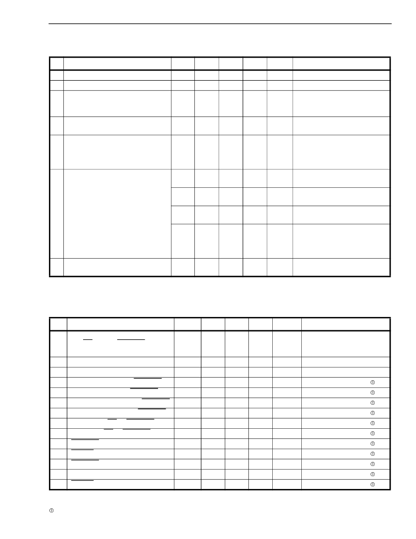
Timing is over recommended temperature range. See Fig. 3 for control and I/O timing details.
Typical figures are at 25°C and are for design aid only; not guaranteed and not subject to production testing.
Crosstalk measurements are for Plastic DIPS only, crosstalk values for PLCC packages are approximately 5dB better.
AC Electrical Characteristics
- Control and I/O Timings
- V
DC
is the external DC offset applied at the analog
I/O pins. Voltages are with respect to V
DD
=5V, V
DC
=0V , V
SS
=-7V, unless otherwise stated.
Timing is over recommended temperature range. See Fig. 3 for control and I/O timing details.
Digital Input rise time (tr) and fall time (tf) = 5ns.
Typical figures are at 25°C and are for design aid only; not guaranteed and not subject to production testing.
Refer to Appendix, Fig. A.7 for test circuit.
AC Electrical Characteristics
- Crosspoint Performance
- V
DC
is the external DC offset at the analog I/O pins.
Voltages are with respect to V
DD
=5V, V
DC
=0V, V
SS
=-7V, unless otherwise stated.
Characteristics
Sym
Min
Typ
Max
Units
Test Conditions
1
2
3
Switch I/O Capacitance
Feedthrough Capacitance
Frequency Response
Channel “ON”
20LOG(V
OUT
/V
Xi
)=-3dB
Total Harmonic Distortion
(See G.5, G.6 in Appendix)
Feedthrough
Channel “OFF”
Feed.=20LOG (V
OUT
/V
Xi
)
(See G.8 in Appendix)
Crosstalk between any two
channels for switches Xi-Yi and
Xj-Yj.
C
S
C
F
F
3dB
20
0.2
45
pF
pF
MHz
f=1 MHz
f=1 MHz
Switch is “ON”; V
INA
= 2Vpp
sinewave; R
L
= 1k
See Appendix, Fig. A.3
Switch is “ON”; V
INA
= 2Vpp
sinewave f= 1kHz
;
R
L
=1k
All Switches “OFF”; V
INA
=
2Vpp sinewave f= 1kHz;
R
L
= 1k
.
See Appendix, Fig. A.4
V
INA
=2Vpp sinewave
f= 10MHz; R
L
= 75
.
V
INA
=2Vpp sinewave
f= 10kHz; R
L
= 600
.
V
INA
=2Vpp sinewave
f= 10kHz; R
L
= 1k
.
V
INA
=2Vpp sinewave
f= 1kHz; R
L
= 10k
.
Refer to Appendix, Fig. A.5
for test circuit.
R
L
=1k
;
C
L
=50pF
4
THD
0.01
%
5
FDT
-95
dB
6
Xtalk=20LOG (V
Yj
/V
Xi
).
(See G.7 in Appendix).
X
talk
-45
dB
-90
dB
-85
dB
-80
dB
7
Propagation delay through
switch
t
PS
30
ns
Characteristics
Sym
Min
Typ
Max
Units
Test Conditions
1
Control Input crosstalk to switch
(for CS, DATA, STROBE,
Address)
Digital Input Capacitance
Switching Frequency
Setup Time DATA to STROBE
Hold Time DATA to STROBE
Setup Time Address to STROBE
Hold Time Address to STROBE
Setup Time CS to STROBE
Hold Time CS to STROBE
STROBE Pulse Width
RESET Pulse Width
STROBE to Switch Status Delay
DATA to Switch Status Delay
RESET to Switch Status Delay
CX
talk
30
mVpp
V
IN
=3V+V
DC
squarewave;
R
IN
=1k
, R
L
=1k
.
See Appendix, Fig. A.6
f=1MHz
2
3
4
5
6
7
8
9
C
DI
F
O
t
DS
t
DH
t
AS
t
AH
t
CSS
t
CSH
t
SPW
t
RPW
t
S
t
D
t
R
10
pF
MHz
ns
ns
ns
ns
ns
ns
ns
ns
ns
ns
ns
20
10
10
10
10
10
10
20
40
R
L
= 1k
,
C
L
=50pF
R
L
= 1k
,
C
L
=50pF
R
L
= 1k
,
C
L
=50pF
R
L
= 1k
,
C
L
=50pF
R
L
= 1k
,
C
L
=50pF
R
L
= 1k
,
C
L
=50pF
R
L
= 1k
,
C
L
=50pF
R
L
= 1k
,
C
L
=50pF
R
L
= 1k
,
C
L
=50pF
R
L
= 1k
,
C
L
=50pF
R
L
= 1k
,
C
L
=50pF
10
11
12
13
14
40
50
35
100
100
100
相關PDF資料 |
PDF描述 |
|---|---|
| MT8809AC | ISO-CMOS 8 x 8 Analog Switch Array |
| MT8809AE | ISO-CMOS 8 x 8 Analog Switch Array |
| MT8809AP | ISO-CMOS 8 x 8 Analog Switch Array |
| MT8812 | ISO-CMOS 8 x 12 Analog Switch Array |
| MT8812AC | ISO-CMOS 8 x 12 Analog Switch Array |
相關代理商/技術參數(shù) |
參數(shù)描述 |
|---|---|
| MT8809AC | 制造商:MITEL 制造商全稱:Mitel Networks Corporation 功能描述:ISO-CMOS 8 x 8 Analog Switch Array |
| MT8809AE | 制造商:Microsemi Corporation 功能描述: |
| MT8809AE1 | 制造商:Microsemi Corporation 功能描述:ANLG AUD/VID CROSSPOINT 45MHZ 8 X 8 28PDIP - Rail/Tube |
| MT8809AP | 制造商:Microsemi Corporation 功能描述:ANLG AUD/VID CROSSPOINT 45MHZ 8 X 8 28PLCC - Rail/Tube |
| MT8809AP1 | 制造商:Microsemi Corporation 功能描述:ANLG AUD/VID CROSSPOINT 45MHZ 8 X 8 28PLCC - Rail/Tube 制造商:MICROSEMI CONSUMER MEDICAL PRODUCT GROUP 功能描述:IC ANLG SWITCH ARRAY 8X8 28PLCC 制造商:Microsemi Corporation 功能描述:IC ANLG SWITCH ARRAY 8X8 28PLCC |
發(fā)布緊急采購,3分鐘左右您將得到回復。